Copper and PTFE stick together to support better 5G
Researchers from Osaka University have demonstrated a method to improve the adhesion of smooth copper foil to PTFE for use in electronic circuits
The amount of digital communication supporting our daily lives continues to increase. This means there is a constant need to improve hardware, including optimizing the performance of printed wiring boards (PWBs). Researchers from Osaka University have demonstrated a method for strongly combining polytetrafluoroethylene (PTFE) and smooth cooper foil. They presented their findings at the INTERFINISH2020 congress.
Because the digital information being transported through communication systems is increasingly complex, the frequency of transmissions must increase. However, as the frequency increases so too does the loss of transmission from the conduction component of the circuit. Therefore, materials must be continually improved to create future-ready PWBs.
Copper is the go-to wiring material for PWBs because it is highly conductive, and thus efficiently transports information to its destination. There is currently nothing superior to copper for this task, so the focus for improvement is to decrease transmission loss from the support material.
PTFE is ideal for this role because it has both low relative dielectric constant and low dielectric loss tangent; however, PTFE does not like to stick to things. An intermediate layer is often used between PTFE and copper to improve the adhesion, but using these layers is a tradeoff because they increase insertion losses.
In this study, the researchers have created an adhesive-free method of sticking commercially available PTFE to copper foil with high adhesion strength, thus dispensing with the need for a middle layer.
“Our technique involves what is known as heat-assisted plasma (HAP) treatment,” explains first author Misa Nishino. “We subjected the PTFE to a HAP to make the surface stickier, and then pressed the two layers together at a high temperature to ensure they were strongly bonded.”
The research team examined pure PTFE and a cloth woven from glass and PTFE and found that both showed significantly increased adhesion to copper foil after HAP treatment. In addition, the very smooth surface of the copper foil meant that the transmission could have an obstruction free pathway, minimizing the losses.
“Our method is both simple and environmentally friendly, making it a highly attractive option for large scale processes,” says study corresponding author Yuji Ohkubo. “We expect our findings will be used to make high-frequency PWBs that will contribute to the enhancement of digital devices for the 5G world and beyond.”

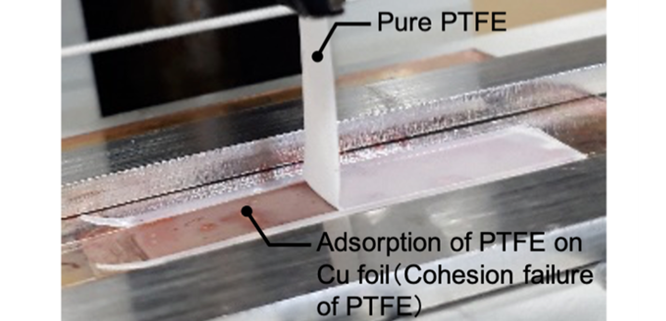
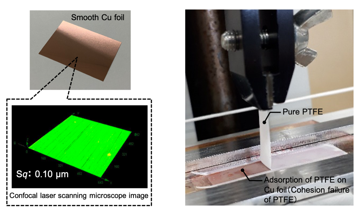
Fig.1 (a) Photograph of the extremely smooth Cu foil and its surface image. (b) Photograph of the Cu foil/PTFE assembly during the 90° peel test

Fig.2 Comparison of the developed printed circuit board and conventional alternatives.

Fig.3 Photographs of Cu foil/pure-PTFE and Cu foil/glass cloth-containing PTFE assemblies before and after the 90° peel test (n = 2).
The study, “Adhesive-free strong adhesion between heat-assisted-plasma (HAP)-treated polytetrafluoroethylene (PTFE) and copper foil,” is presented at the INTERFINISH2020 congress from Sep. 6-8th in 2021.
Related Links
Endo Lab., Research Center for Precision Engineering, Graduate School of Engineering, Osaka University
OHKUBO Yuji (Researchers Database)
nanoManufacturing Science Lab. (Yamamura Lab.), Department of Precision Engineering, Graduate School of Engineering, Osaka University
Yamamura Kazuya (Researchers Database)
Past Articles
Success in affixing fluoropolymer to Isobtylene-isoprene Rubber without using adhesive [9/8/2014]
A technique enabling fluorine-containing resin to adhere strongly to a metal film without using adhesive [1/19/2016]
Lifetime of surface modification of polytetrafluoroethylene (PTFE) extended [1/25/2017]
Give It the Plasma Treatment: Strong Adhesion without Adhesives [12/25/2018]
