
Success in developing a simple method for fabricating single-layer graphene nanoribbons from double-walled carbon nanotubes
Will lead to increased performance of nanodevice circuits
A research group led by Prof. TANAKA Hirofumi of the Graduate School of Engineering, Osaka University (visiting professor from Kyushu Institute of Technology), in collaboration with a research team comprised of Prof. OGAWA Takuji and Prof. KOBAYASHI Yoshihiro of Osaka University, Prof. KASAI Seiya of Hokkaido University, and Associate Prof. YAMADA Toyokazu of Chiba University, succeeded in (1) finding a method to fabricate single-layer graphene nanoribbon (sGNR) by an unzip of double walled carbon nanotube (DWNT) and (2) discovering that the electric property of sGNR could be controlled by the adsorption of nanoparticles of planar molecules and that sGNR changes to semiconducting only near the area of adsorption. As known in "Moore´s Law," the downsizing of nanodevices is nearing its physical fabrication limit.
The phenomena found in this work will help speed up the information process in devices of the same size to current Si devices.

Fig.1. Fabrication process to obtain single layer graphene nanoribbons (sGNR). Blue and red sheet corresponds to single carbon atomic layer each.
(a) defect induce by anneal(b) Unzip by sonication. Unzip start from the defects. (c) DWNT was perfect unzip.(d) flat double layer GNR(dGNR)was
obtained.(e) further sonication promote separation of dGNR (f) two single layer GNR(sGNR)were finally obtained. sGNR obtained from outer wall (red) is slightly wider than that from inner wall (blue).

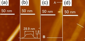
Fig.2. AFM images of (a) pristine DWNT (b) obtained dGNR by unzipping (c) Separation area of two GNRs from dGNR (d) obtained sGNR. Each scale bar indicates 50nm (e) Line profile of dGNR in (c).Line profile in (a), (b), (d) were obtained along the line in images.(a)-(d)were obtained by different samples.

Fig.3. (a)molecular structure of NDI (b) AFM image after adsorption of NDI nanoparticles (c) Gate property of FET structure of GNR/NDI complex. After adsorption of NDI nanoparticles, sGNR changed to p-semiconductor. Inset show structure of back-gate FET. (d)Model of neck structure and hole injection induced by NDI nanoparticles.
To learn more about this research, please view the full research report entitled " Method for Controlling Electrical Properties of Single-Layer Graphene Nanoribbons via Adsorbed Planar Molecular Nanoparticles " at this page of the Scientific Reports website.
Related Links