Current events: Improved reliability of printed circuit boards
Researchers from The Institute of Scientific and Industrial Research (SANKEN) at Osaka University optimized the interfaces that are foundational to the electrical connections in advanced printed circuit boards. This work will improve the functional lifetime of modern electronics
The function of consumer electronics, airplanes, and a vast number of other technologies depend on properly constructed printed circuit boards. These are devices that hold electrical parts together and ensure proper electrical connections. Microvias are small components that provide these electrical connections, and are especially important for the high-density circuitry that's central to the portability and functionality of advanced electronics. A common reason why such circuitry fails is deterioration of the microvias. An improved method of fabricating microvias would enhance the reliability of modern electronic devices.
Now, in a study recently presented in Surface Mount Technology Association International Virtual Conference 2021 and International Conference on Device Packaging 2022, researchers from Osaka University have studied such a method—termed FLET, which eliminates the void spaces that are a common reason for printed circuit board failure. This study will improve the reliability of a technology that's foundational to the long life of household, medical, and many other technologies.
Copper microvias are fabricated by a straightforward chemical reaction: reduction of copper ions into copper metal—i.e., copper plating—by using formaldehyde in base. "The problem here is hydrogen production, a chemical byproduct during the copper plating," explains Katsuaki Suganuma, senior author. "Hydrogen accumulation leads to bubbles, nano-sized voids, which weaken the mechanical properties of the microvias—especially under thermal stress."
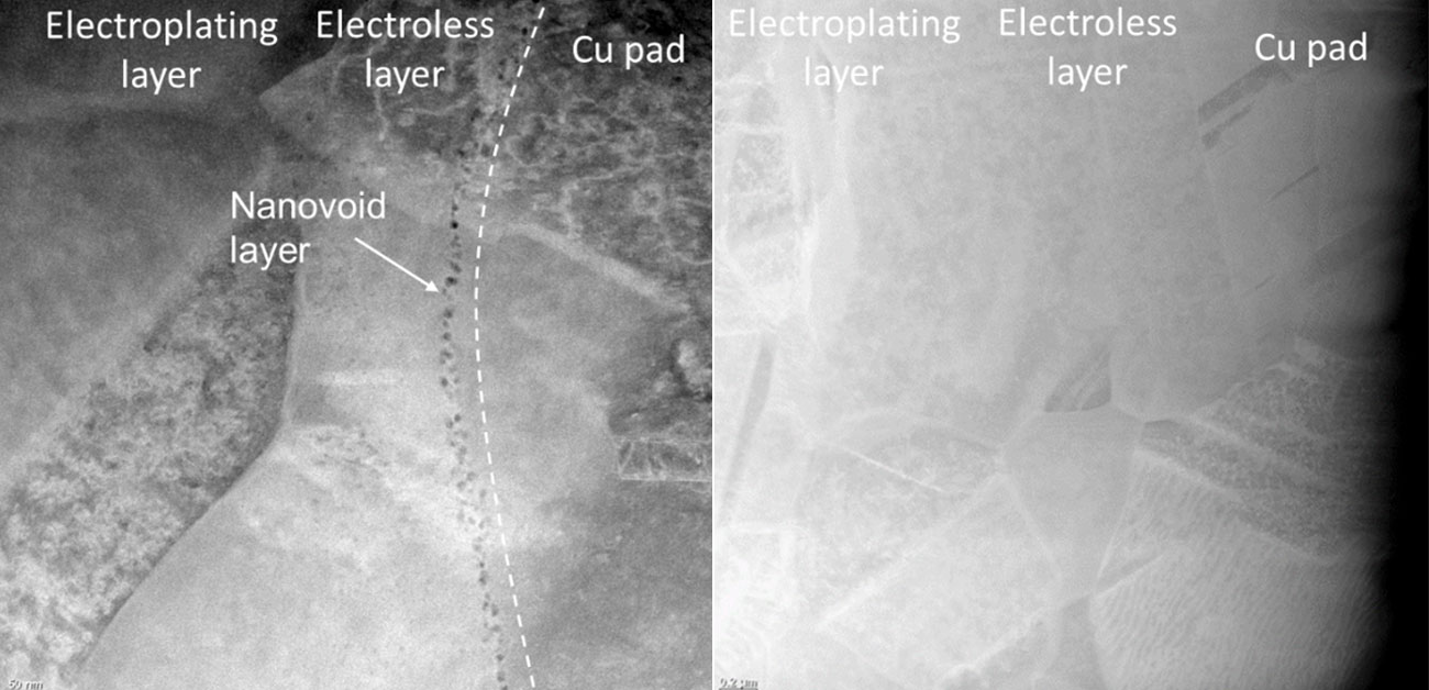
To help prevent formation of microvias, FLET makes two changes to the standard microvia fabrication protocol. One change is to reduce—by a factor of 20—the extent of surface roughening of the copper surface onto which the microvias are deposited. Another change is to not use a nickel reductant. Microscopic imaging provided clear evidence for the success of FLET. By the traditional method, clear nano-sized voids were present at the newly formed copper–copper interface, and the microstructure was irregular. By FLET, nano-sized voids were not evident and the microstructure was continuous.
"This is clear evidence that by FLET, hydrogen bubbles did not disrupt the integrity of the copper–copper interface, and that deposition was epitaxial," says Zheng. "In other words, delamination, cracking, and other failures are less likely." Nevertheless, the exact mechanism of the improvement facilitated by FLET requires further research.
This study reports a straightforward means of improving electrical interconnects in high-density circuitry, in a manner that does not substantially change well-established, trusted protocols. Thus, the results of Zheng and colleagues should help FLET gain acceptance in industry for improving the lifetime of both standard and specialized electronics.
Fig. 1 SEM image of a microvia structure in a commercial PCB substrate (left) and TEM image of the interface at the electroless Cu area (right).
Original content, Katsuaki Suganuma, Credit must be given to the creator.
Fig. 2 STEM image of the microvia structure in the conventional Cu electroless plating method (left); and the Cu, Ni, O, and Pd elemental distributions in the area of electroless Cu plating (right).
Original content, Katsuaki Suganuma, Credit must be given to the creator.
Fig. 3 Comparison of the microvia structure at the interface by the conventional (left) and FLET Cu electroless (right) methods.
Original content, Katsuaki Suganuma, Credit must be given to the creator.
The study, “Improvement of micro-via reliability by using a new electroless Cu plating” was presented in International Conference on Device Packaging 2022.