A golden ticket to smaller electronics
Researchers at Osaka University demonstrate a new method for creating three-dimensional integrated circuit connections that works at low temperatures and does not require external pressure, which may lead to inexpensive and energy efficient electronic devices
Scientists from the Flexible 3D-System Integration Laboratory at Osaka University developed a new method for the direct three-dimensional bonding of copper electrodes using silver, which can reduce the cost and energy requirements of new electronic devices. This work may help in the design of next-generation smart devices that are more compact and use less electricity.
Three-dimensional integrated circuits are playing an increasingly important role in electronic devices. Compared with conventional 2D circuits, these architectures can save both space and reduce the material required for interconnecting wires. However, the ability to form reliable 3D connections requires new methods compared with the mature technologies in use for convention integrated circuits.
Now, a team of researchers at Osaka University showed how to directly connect copper electrode “bumps” using silver layers. “Our process can be performed under gentle conditions, at relatively low temperatures and without added pressure, but the bonds were able to withstand over one thousand cycles of thermal shocking from -55 to 125 ºC,” first author Zheng Zhang says. In this new method, silver is first sputtered onto the two copper surfaces to be bonded at room temperature. Then, heat was applied to anneal the silver layers, which caused the surface to undergo microscopic changes in a process called “stress migration”. The release of the stress during annealing led to surface roughening, which ensured a sufficient effective area between the two silver layers. As a result, bonding could be accomplished without applied pressure even at a comparative low annealing temperature. Permanent connections as small as 20 micrometers could be realized in just ten minutes this way. This process also requires only moderate temperatures (180 °C) and can work under atmospheric conditions.
The team was able to confirm the surface roughness of the sputtered and annealed chips using images from by scanning electron microscopy and atomic force microscopy. “This technology is expected to contribute to chips with a high density of interconnects and advanced 3D packaging,” senior author Katsuaki Suganuma says.
Fig.1 (Right) SEM image of fabricated 20-μm Cu-Ag bumps, (Middle) Schematic drawing of the prepared bump cross-section, (Left) Schematic drawing of the bonded 20-μm Cu-Ag bump device.
Original content
Katsuaki Suganuma
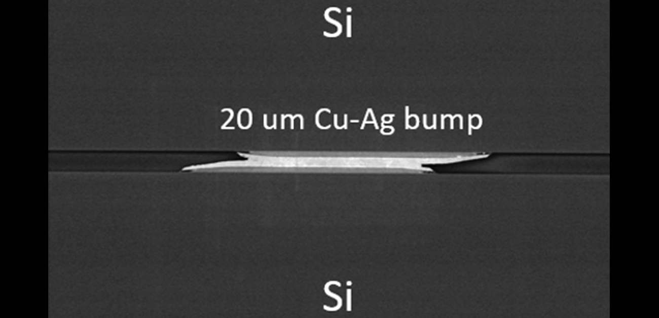
Fig.2 (Right) Cross-sectional image of bonded Cu-Ag bump, (Left) Magnified view of the interface of the bonded Cu-Ag sample.
Original Content
Katsuaki Suganuma
The study, “Ag-Ag direct bonding via a pressureless, low-temperature, and atmospheric stress migration bonding method for 3D integration packaging,” was presented in EEE 72nd Electronic Components and Technology Conference (ECTC).
Related Links
F3D website (link in Japanese)