(Noise-) Less is More
Development of high precision 3D circuit simulator allows for electromagnetic noise-less circuit layout
A group of researchers from Osaka University led by Prof. Masayuki Abe and Prof. Hiroshi Toki of the Graduate School of Engineering Science developed a high precision 3D circuit simulator in the time-domain for quantifying electromagnetic (EM) noise and elucidated its origin, allowing for electronic and electrical circuit layout to reduce EM noise.
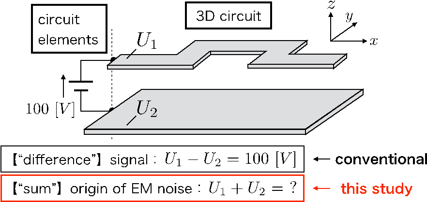
In our day-to-day lives, ordinary electrical appliances start up when plugged into a voltage outlet. When an appliance is plugged in, the “difference” of potential is applied to the plug, and the electrical circuit in the product is driven. However, EM noise originates from the “sum” of potentials, something to which we do not normally pay much attention. Since it is difficult to visualize why, where, and when the “sum” of potential generates in electrical circuits, noise treatments are given based simply on know-how. The results of this research have made it possible to quantify not only the “difference” of physical quantity, which is normally used in conventional circuit theory, but also the “sum” of physical quantity, which can act as the origin of EM noise phenomena (Fig.1). As our lives are becoming more and more convenient due to the spread of devices powered by electricity, the risk of problems caused by EM noise has also increased. Therefore, visualizing the generation process of EM noise and understanding how it occurs are very important in cutting-edge circuit design.
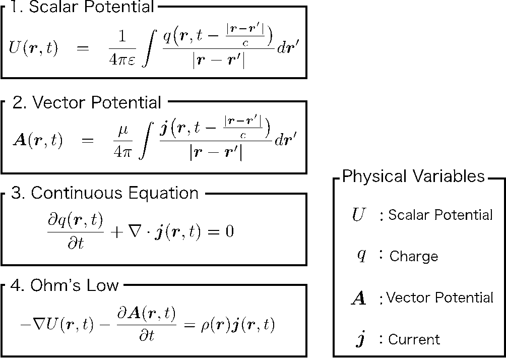
In this study, the group developed a calculation method for quantifying the “sum” of physical quantities, which causes EM noise, as well as a simulator that can visualize the origin of the noise phenomenon. Specifically, they were able to directly calculate the simultaneous partial differential integral equation with the variables of scalar potential, charge, vector potential, and current, which are EM physical quantities in the three-dimensional conductors constituting the circuit (Fig.2). Furthermore, the group developed an algorithm that connects circuit elements (voltage sources, resistors, etc.) at arbitrary boundaries as inputs. The method developed in this research makes it possible to visualize how physical quantities in electrical conducting materials propagate and change over time (see the Supplementary Information section at this link: https://www.nature.com/articles/s41598-019-53288-x ). As a result, it is possible to intuitively understand why, where, and when EM noise is generated, and develop a circuit design that fundamentally eliminates the origin of EM noise.
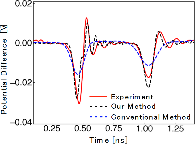
This method also considers the conductor shape that determines circuit characteristics with high accuracy. In the demonstration experiment, the calculation technology developed in this study was observed to closely reproduce the waveform of the experiment (Fig.3). In the future, the group will use this research technology to elucidate the EM noise phenomenon caused by the “sum” of potentials generated in various commonly-used circuit conductors and apply the findings to noiseless circuit design.
The research group is aiming to realize a “noiseless” society, and expect that their theories and calculations can lead to noiseless equipment with low power consumption. They are actively pursuing endeavors to realize a noiseless infrastructure and want to conduct both basic and applied research on EM noise toward the social implementation of equipment that reduces EM noise. Prof. Abe and Prof. Toki are looking for partners from the industrial realm in various fields for everything from basic research to applied development.

Fig.1
Schematic diagram used in this study. The time variation of physical quantity in a three-dimensional circuit conductor with circuit elements (the figure is a plane (2D) but can also be 3D configuration). In addition, the sum component that is the origin of electromagnetic noise can be quantified.

Fig.2
Equations and variables used in this study. The physical quantity used in electromagnetism is calculated as a variable. Equations 1 and 2 represent the potential obtained from Maxwell's equations, the sources of which are charge and current. In addition, the relationship between current and charge is expressed using continuous equation in Eq.3, and the relationship between potential and current is expressed using Ohm's law in Eq. 4. By solving these equations simultaneously, phenomena in the circuit can be described.

Fig.3
Experimental results and numerical calculation results obtained by this research method and conventional methods. When the potential difference is 0, the EM noise is not generated, and the generated potential difference indicates the EM generated by bending the wiring of the circuit. It can be seen that this research method reproduces the experiment with high accuracy.
The article “Time-domain formulation of a multi-layer plane circuit coupled with lumped-parameter circuits using Maxwell equations,” was published on November 29 in Scientific Reports at DOI: https://doi.org/10.1038/s41598-019-53288-x .
Related links
