
Promising technology for manufacture of electronic devices
A group of researchers from Osaka University, The University of Tokyo, and RIKEN have clarified that the structure of the surface of an organic semiconductor differs completely from the structure of its bulk.
• Osaka University -- WAKABAYASHI Yusuke (Associate Professor)
• The University of Tokyo -- TAKEYA Junichi (Professor), HOTTA Chisa (Associate Professor)
• RIKEN -- KORETSUNE Takashi (Sernior Fellow)
Many electronic devices are made taking advantage of the special properties of interfaces. Thus, in order to make more advanced high-performance devices, designing and making interfaces possessing the desired properties is a necessity. To make such desired properties, the structure of the interface needs to be tailored.
Generally, the atomic structure at the surface and interface of matter is different from that of the bulk.This phenomena is called "surface relaxation" or "surface reconstruction" and the surface of metals and silicon has been studied extensively. Organic devices are expected to have greater surface relaxation because of the weak inter-molecular interactions of their material; however, as organic matter possesses very complicated structures, the "relaxation" of these surface structures has not been studied.
Inexpensive and light organic semiconductors are in practical use in organic light-emitting diode displays. In transistors made with organic semiconductors instead of silicon, the carriers usually transfer within the first few molecular layers; however, how molecules are arranged in such small regions on the surface has been unknown.
Using radiation light at the Photon Factory (PF), High Energy Accelerator Research Organization (KEK) and a unique analyzing method using holography, this group has found that molecular arrangements at the surface layer are completely different from that of the bulk. Furthermore, using theoretical calculations, this group has confirmed that this difference causes a difference in electric conductivity between the surface and the bulk of the semiconductor.
This change in surface structure found by this group has demonstrated that an ultra-thin film possessing a self-repairing function could be produced on the surface of semiconductors. This group's results will lead to the development of techniques for manufacturing precise and stable micro devices for controlling conductivity at the molecular layer level by selecting molecules for use.
Abstract
Organic crystals are likely to have a large degree of structural relaxation near their surfaces because of the weak inter-molecular interactions. The design of organic field-effect transistors requires a detailed knowledge of the surface relaxation as the carriers usually transfer within the first few molecular layers at the semiconductor surfaces, and their transport properties reflect the structural changes through the transfer integral. Here, we report the direct observation of the surface relaxation of an organic semiconductor, a tetracene single crystal, by means of X-ray crystal truncation rod scattering measurements. A significant degree of surface relaxation is observed, taking place only in the first monolayer at the semiconductor surface. First principles calculations show that the resultant transfer integrals are completely different between the bulk and surface of the semiconductor.
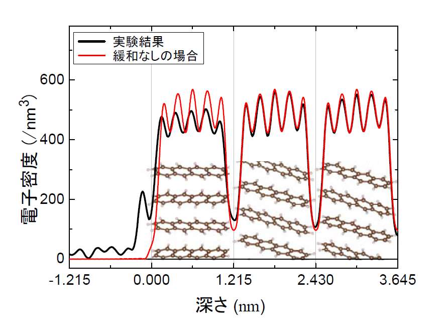
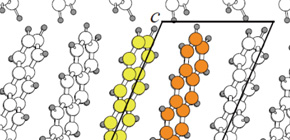
Figure 1
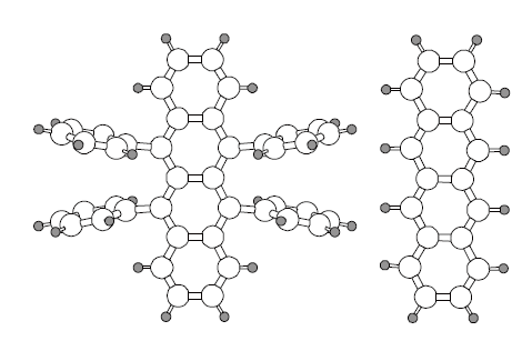
Figure 2
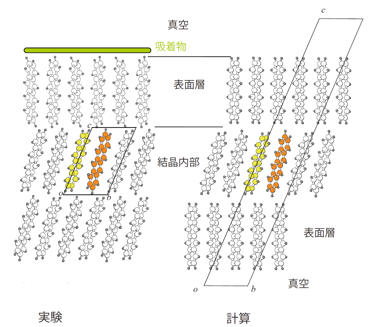
Figure 3
To learn more about this research, please view the full research report entitled " Large surface relaxation in the organic semiconductor tetracene " at this page of the Nature Communications website.
Related Link