
Silicon nanoblock arrays create vivid colors with subwavelength resolution
Osaka University researchers demonstrate a silicon metamaterial surface that will allow for color printing with diffraction-limited resolution
Until now, the metamaterials used to create tunable color from structural geometry have been based on metals. Although effective in achieving high resolutions, metallic materials suffer from inherent energy losses at visible wavelengths, which makes optimizing color purity challenging. By comparison, the resonance of silicon materials enables high reflectance and purity.
A trio of researchers at Osaka University recently demonstrated precise color control using monocrystalline silicon. Their colorful findings were published in Nano Letters .
“The use of silicon allows us to achieve both high resolution and high saturation,” study corresponding author Junichi Takahara says. “All-dielectric materials that can produce individual color pixels with high-resolution, without color mixing, offer distinct advantages over metallic materials.”
The metamaterial arrays feature nanoscale patterns that function as antennae, which convert optical radiation into localized energy. Electron beam lithography was used to create masks, which were used to protect the silicon surface from subsequent plasma etching. The team was able to generate vivid colors controlled completely by the geometry of the antennae, also demonstrating white light generation, which is important for full-color printing. In addition, two-color information was inherent in each pixel and could be revealed by changing the polarization of the incident light.
The subwavelength resolution was demonstrated by generating a clearly discernable yellow and blue checkerboard pattern within unit areas of just 300×300 nanometers. In terms of eventual applications, this translates into printing at ~85,000 dpi.
The team also had some fun demonstrating their control with some nanoscale color-appropriate typography, writing “RGB” in the necessary width nanoblocks to generate a striking effect.
“Our work reveals the high degree of precision possible through etching monocrystalline silicon,” lead author Yusuke Nagasaki says. “The agreement between the calculated and experimental reflectance values for our system also supports our confidence in the robust nature of the technique we created.”
The dual-color properties of the pixels offer the potential to create overlaid images, as well as maximizing the information encoded into a particular area of the array. The work shows potential for use in anti-counterfeiting technology and advanced display technology such as three-dimensional displays.

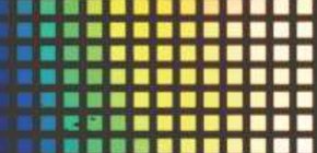
Fig. 1.
Bright-field optical microscope image of the Si nanostructure arrays. Si nanostructures of different sizes exhibit distinct reflection colors. (scale bar is 20 μm).
(©2017 Takahara et al. Nano Letters. 17, 7500-7506. DOI: 10.1021/acs.nano-lett.7b03421)
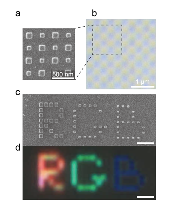
Fig. 2
. Demonstration of a subwavelength pixel. (a) Scanning ion and (b) optical microscope images of a checkered pattern consisting of alternating nanoblocks of two different sizes. (c) Scanning ion and (d) optical microscope images of the letters “RGB” by means of Si nanostructures generating the corresponding color. (scale bar is 2 μm).
(©2017 Takahara et al. Nano Letters. 17, 7500-7506. DOI: 10.1021/acs.nano-lett.7b03421)
To learn more about this research, please view the full research report entitled " All-Dielectric Dual-Color Pixel with Subwavelength Resolution " at this page of Nano Letters .
Related link