
Development of Nanostructuring Technology to Simultaneously Control Heat and Electricity
The improvement of thermoelectric materials that can directly convert wasted heat to electric energy may lead to one of the solutions for energy issues. For high performance in thermoelectric materials, it’s required to easily conduct electricity while making it difficult for heat to pass through. Namely, high electrical conductivity and low thermal conductivity are needed. However, it has been very difficult for long because both conductivities are correlated. Now, nanostructuring was expected for the independent control of both conductions, but its methodology by nanostructuring was still unclear.
Yoshiaki Nakamura, Professor of Osaka University proposed a unique nanostructure (Fig. 1) and established a methodology for the development of a material in which heat and electricity conductions can be controlled simultaneously.
His research group created a nanostructure in which ultrasmall germanium (Ge) nanodots were formed with identical crystal orientations in silicon (Si). In this structure, electric currenct flows in Si and thermal conduction was prevented by Ge nanodots, therefore, high electric conductivity and low heat conductivity were realized simultaneously. By making the shape and dimension of Ge nanodots control factors, it has become possible to control thermal conductivity at will. Using this technique, this group succeeded in increasing Si/Ge interfacial thermal resistance by 2 to 3 times of conventional figures, gaining the largest Si/Ge interfacial thermal resistance in the world.
The results of this research show that by introducing epitaxially-grown ultrasmall Ge nanodots into materials with high electric conductivity, the conduction of heat and electricity can be successfully controlled simultaneously. In addition, because these results are not limited to Si, one can anticipate that this research will be employed in the development of thermoelectric materials that utilize other materials as well, which are in high demand for waste heat utilization in factories and automobiles.
In our present information society, the waste heat given off by the LSI (Large scale integrated circuits) in our PCs and servers has grown massive over the years, and the development of Si-based thermoelectric materials compatible with LSI has become necessary in order to utilize this waste heat as thermoelectric power. This research has shown a possible improvement of the efficiency of this conversion of waste heat to electricity through introducing nanostructures to Si, a potential breakthrough in the realization of Si-based thermoelectric materials for use in LSI waste heat conversion.
The results of this research were published in Scientific Reports on Monday 5 October 2015.
Abstract
Phonon transport in Si films was controlled using epitaxially-grown ultrasmall Ge nanodots (NDs) with ultrahigh density for the purpose of developing Si-based thermoelectric materials.
The Si/Ge ND stacked structures, which were formed by the ultrathin SiO2 film technique, exhibited lower thermal conductivities than those of the conventional nanostructured SiGe bulk alloys, despite the stacked structures having a smaller Ge fraction. This came from the large thermal resistance caused by phonon scattering at the Si/Ge ND interfaces. The phonon scattering can be controlled by the Ge ND structure, which was independent of Si layer structure for carrier transport.
These results demonstrate the effectiveness of ultrasmall epitaxial Ge NDs as phonon scattering sources, opening up a route for the realisation of Si-based thermoelectric materials.
Fig.1 Schematic of Si/Ge nanodot stacked structure and carrier and phonon transports.
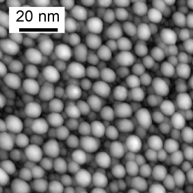
Fig. 2 Scanning tunneling micrscope image of ultrasmall Ge nanodots formed by our technique.
Fig. 3 The dependence of the thermal resistance per cycle on the nanodot size.
Fig. 4 Thermal conductivity of our nanoarchitecture and the conventional SiGe materials.
To learn more about this research, please view the full research report entitled " Phonon transport control by nanoarchitecture including epitaxial Ge nanodots for Si-based thermoelectric materials " at this page of the Nature's Scientific Reports website.
Related links