
New strain gauge: 200-fold improvment of sensitivity
A big step toward health monitoring of building structures and biosignals
The Institute of Scientific and Industrial Research of Osaka University, in cooperation with University of Genoa (Italy) and the CNR-SPIN Institute (Italy), has developed a strain gauge with the highest strain sensitivity of 400.
A strain gauge is a sensor used to measure strain on an object. Deformation of the object causes its electrical resistance to change. A fundamental parameter of the strain gauge is its sensitivity to strain, expressed quantitatively as the gauge factor (GF). The GF is defined as the ratio of fractional change in electrical resistance to the fractional change in length (strain). In industrial applications, nickel alloys are used as a strain-detecting material. Since the GF of nickel alloys is a low figure of 2, efforts to increase the sensitivity of circuits used for strain measurements have been made by boosting the signal level to increase measurement resolution and reducing noise.
Since the newly developed strain gauge allows for microstrain detection without amplifying signals, it will miniaturize electrical circuits used for measuring unknown electrical resistance and reduce energy consumption.
In order to detect microstrain with a strain gauge, it is necessary to develop materials with a high GF. This joint group has developed highly sensitive strain gauges using vanadium dioxide (VO 2 ). VO 2 exhibits a typical metal-to-insulator phase transition (MIT) via the strong coupling of strain, thermal, optical, and dielectric stimuli. The MIT accompanies a sharp change in electrical resistance and optical change in the infrared region. Thus, VO 2 has potential applications, such as switches, infrared sensors, and smart windows, attracting widespread attention.
To use VO 2 for electronic devices, it is necessary to grow its thin film on a substrate. Because the MIT aspect in VO 2 thin films is closely related to crystallinity and strain direction, the single crystal growth of VO 2 thin films had been a longstanding target.
In this study, in addition to the formation of a single-crystal micromesh VO 2 thin film on a flexible polymer [poly(dimethylsiloxane); PDMS], the separation of the mesh-patterned VO 2 thin film from the MgO substrate and the transfer of the film to PDMS led to the development of this flexible strain sensor with the highest GF of 400.
The single-crystal strain gauge offers greater sensitivities to the GF. In experiments, the temperature dependence of the resistance curve in a single-crystal VO 2 thin film was shown and the change in resistance of 3 orders of magnitude was clearly confirmed.
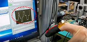
The technique for fabricating oxide ceramic thin films on flexible substrates is widely used and can be applied to high-temperature superconductors and magnetic materials. This strain gauge, which enables detection of µε (microstrain), the elongation and contraction of 1 µm (0.000001 m) per 1 m length, will lead to the development of simple devices for measuring pulse waves, muscle movement, and aging degradation of buildings and bridges in the future.

Figure 1
To learn more about this research, please view the full research report entitled "Formation of single-crystal VO 2 thin films on MgO(110) substrates using ultrathin TiO 2 buffer layers" at this page of the Applied Physics Express website.
Related Links