
Silicon thermoelectric nanomaterials with minimum thermal conductivity achieved
Recycling exhaust heat as electric energy has entered the realm of possibility
A group of researchers developed a technique for creating thermoelectric materials by assembling nanocrystals with oriented crystals. Researchers involved in this achievement were:
• Graduate School of Engineering Science, Osaka University -- Associate Professor Yoshiaki NAKAMURA , Assistant Professor Jun KIKKAWA (currently, Chief researcher, NIMS), Professor Akira SAKAI
•The University of Tokyo -- Associate Professor Jun-ichiro SHIOMI
• Advance Riko Inc. (former ULVAC, Inc.) -- Dr. Satoaki IKEUCHI
By making use of this assembly technique, they succeeded in preventing electrical conductivity from deteriorating and reduced thermal conductivity to about one 200th of bulk silicon (Si), the smallest value in the world. In thermoelectric (TE) materials converting exhaust heat energy into electrical energy, heavy elements such as rare metals or materials containing toxic elements have been the norm. Thus, low-priced and environmentally-friendly materials have been demanded.
This group, without the use of rare metals, achieved properties necessary for achieving high-TE-performance, that is, high electrical conductivity and low thermal conductivity, by assembling nanocrystals with oriented crystals. It has been impossible to make such nanostructures by conventional methods.
By making use of their unique nanostructuring technique, this group succeeded in suppressing the deterioration of electrical conductivity and in reducing thermal conductivity to part of 200th of bulk Si, obtaining the minimum value for Si thermal conductivity.
This group's results demonstrate that the realization of environmentally-friendly and low-cost TE materials using Si, an abundant and ecofriendly element, is within the realm of possibility. If Si, an excellent material for making electronic elements, can be made with high TE function, it will become possible to make devices consisting of electronic element materials and TE materials and to recycle exhaust heat from computers and servers as electrical energy. In the sensor network society of the future, this group's technique will possibly become a solution for energy supply to electronic devices in sensors and other items installed in various places.
Abstract
Reduction of thermal conductivity κ while preserving high electrical conductivity σ in materials continues to be a vital goal in thermoelectric study for the reuse of exhaust heat energy. In the use of an eco-friendly and ubiquitous element, Si as thermoelectric material, high κ value in bulk Si is the essential bottleneck to achieve high dimensionless figure of merit. This is a motivation for many recent studies on reducing κ in Si, by nanostructuring, e.g., using grains/wires with size smaller than the phonon mean free path. However, κ reduction that can be achieved tends to be saturated presumably due to an amorphous limit. Here, we present a nanoarchitecture for defeating the κ amorphous limit while preserving bulk-like σ. This new nanoarchitecture is an assembly of Si nanocrystals with oriented crystals separated by a 1-monolayer amorphous layer with well-controlled nanoscale shaped interfaces. At these interfaces, novel phonon scattering occurs resulting in κ reduction below the amorphous limit. Preservation of bulk-like σ results from the coherency of the carrier wavefunctions among the oriented nanocrystals separated by the ultrathin amorphous layer. The results will bring environmentally-friendly and low-cost thermoelectric Si material compatible with mature LSI process technology and represent guidelines for optimized thermoelectric nanostructures.
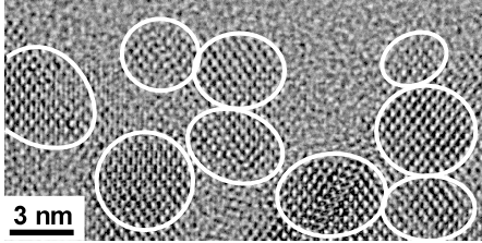
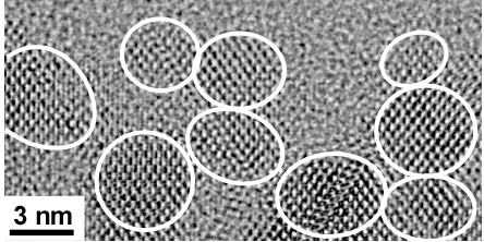
Figure 1. Cross-sectional transmission electron microscope image of connected Si nanodot crystals. Connected Si nanodot crystals with about 3 nm diameter.
Figure 2. Schematic of carrier transport and phonon transport in connected Si nanodot crystals. Schematics of connected Si nanodot crystals and of the transports of carriers and phonons in this structure.
Figure 3. Thermal conductivities of our connected Si nanodot crystals and conventional Si materials. Comparison of thermal conductivities between our connected Si nanodot crystals (this work) and conventional Si materials. Thermal conductivity of our crystal exhibits 0.78 ± 0.12 Wm-1K-1 which is the world’s smallest value.
Figure 4. Thermal resistance per one interface between Si crystal layer/SiO 2 . Thermal resistance per one interface between Si crystal layer/SiO 2 of connected Si nanodot crystals (this work). Calculated thermal resistance per one interface between Si crystal layer/SiO 2 in suppler lattice of Si/ SiO 2 (Calculations 1 and 2). Calculation 1 is done by solving transport equation of phonon with certain energy statistically. Calculation 2 is done using thermal resistance of Si and SiO 2 and interfacial thermal resistance of Si/ SiO 2 .
To learn more about this research, please view the full research report entitled " Anomalous reduction of thermal conductivity in coherent nanocrystal architecture for silicon thermoelectric material " at the Science Direct website.
Related Link