About this research

NAKAMURA Atsutomo
- Graduate School of Engineering Science
- Professor
Atomic Step–Terrace Ordering Enables Unprecedented Precision in Mechanical Testing
Scientists elucidate how atomic-scale surface structure governs deformation at the nanoscale.
As modern technologies shrink to the nanoscale, surfaces increasingly dictate how materials deform, yield, and fail. Yet probing this regime has long been hindered by the challenge of preparing and controlling surfaces with true atomic precision, particularly at the outermost atomic layer.
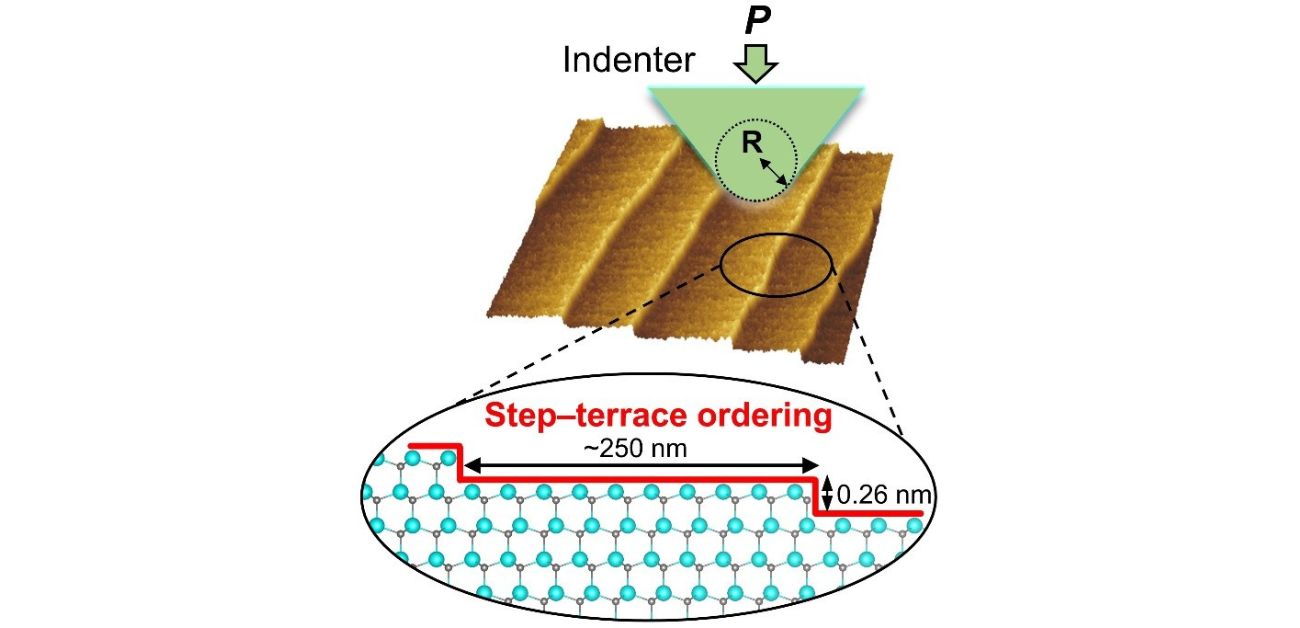
In a recent study published in Small, researchers from The University of Osaka report the creation of step–terrace–ordered GaN surfaces using catalyst-referred etching (CARE). Mechanical testing on these surfaces demonstrates exceptional reproducibility across 100 measurements, achieving record-low stress scatter.
“Surfaces matter more than you think,” says co-first author and Assistant Professor Yan Li. “Conventional roughness metrics in nanomechanical testing should be re-examined. A surface that is only apparently flat is not the same as a surface whose atomic arrangement is ordered down to the outermost atomic layer. In nanoscale mechanical testing, even slight disorder in this outermost layer can lead to scatter in the measured yield response.”
The researchers analyzed 100 load-displacement curves for each of three GaN single-crystal surfaces: CARE-treated, as-received, and mechanically buffed. The CARE-treated surface, featuring well-ordered monoatomic steps and atomically flat terraces, showed striking reproducibility. The relative standard deviation of stress was just 2.3% across 100 tests, representing the lowest scatter reported to date for nanoindentation-based evaluation of the onset of yielding.
By contrast, commercially available GaN substrates (as-received), typically produced by chemo-mechanical polishing, appear smooth at the microscale but retain multi-atomic steps and subtle atomic-scale irregularities at the outermost surface. These hidden features can induce local stress concentration or relaxation, thereby increasing scatter in the measured onset of yielding. The study shows that terrace roughening and multi-atomic steps at the outermost surface significantly perturb the onset of plasticity. In mechanically buffed surfaces, near-surface dislocations introduced by polishing further reduce reproducibility by facilitating plastic deformation at lower and less uniform stresses.
“Specimen preparation is as important as the testing method itself,” explains corresponding author Professor Atsutomo Nakamura. “By ordering the surface atomic structure of GaN crystals, we could evaluate the onset of yielding with unprecedented precision. This work provides a new criterion for nanoscale mechanical testing that goes beyond conventional roughness-based evaluation.”
The implications extend beyond GaN. In semiconductors, ceramics, metals, and functional crystals, nanoscale reliability depends on how precisely the onset of deformation can be evaluated. For practical technologies such as integrated circuits, optoelectronic devices, and micro-electro-mechanical systems (MEMS), hidden disorder at the outermost surface may introduce unexpected reliability issues. The study provides a framework for improving surface processing, quality control, materials design, and reliability assessment.
Fig. 1 Measuring the onset of yielding on the CARE-treated GaN surface. The well-ordered step-terrace structure on the surface is also shown.
Credit: The University of Osaka
Fig. 2
Caption: One hundred tests on the CARE-treated GaN surface demonstrate exceptional repeatability, with unprecedentedly low scatter in the measured onset of yielding.
Credit: The University of Osaka
Fig. 3
Caption: Local convex or concave features on the surface lead to stress concentration or relaxation.
Credit: The University of Osaka
Note
The article, “Atomic Step-Terrace Ordering Enables Unprecedentedly Low Pop-in Stress Scatter in GaN (0001)”, was published in Small on April 27, 2026 at DOI: https://doi.org/10.1002/smll.202512390