Bringing real-time, fine-scale, subsurface quality control to 3D printing
Researchers from Osaka University used laser ultrasonics to image ultrasmall internal defects in 3D-printed materials, thus introducing a means of non-contact quality control
3D printing is revolutionizing manufacturing by wasting much less material and energy than that by conventional machining and production line assembly. Now, researchers from Japan have made a discovery that will help companies reliably make even highly complex 3D-printed products.
In a study recently published in Ultrasonics, researchers from Osaka University used laser ultrasonics to detect fine-scale defects below the surface of 3D-printed metal assemblies, and in so doing have introduced a unique quality control technology to the field of 3D printing.
Machining has long been the primary method to make products. The basic idea is that you start with a larger piece of material, cut it into a specific shape, and then assemble separately prepared parts into a larger product. With machining, quality control checks can be performed at each step of the manufacturing process, but it's difficult to rapidly build a prototype or a highly complex product. In these instances, a more useful approach is 3D printing: layer-by-layer assembly starting from (for example) a computerized blueprint. Overcoming the challenges of 3D printing—such as the difficulty of detecting internal defects without damaging the product—is something the researchers at Osaka University aimed to address.
"It is often challenging to use laser-generated ultrasonic echoes for identifying subsurface defects in 3D-printed devices," explains lead author of the study Takahiro Hayashi. "We generated ultrasonic waves in the megahertz range to uncover small defects that are frequently difficult to image."
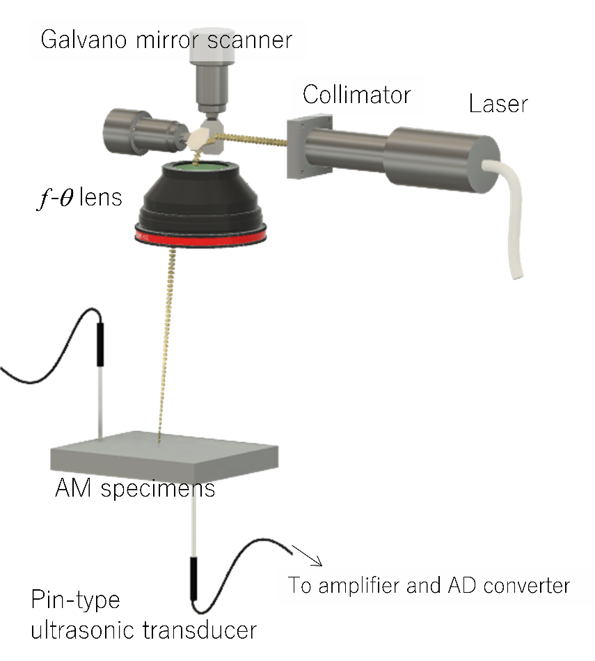
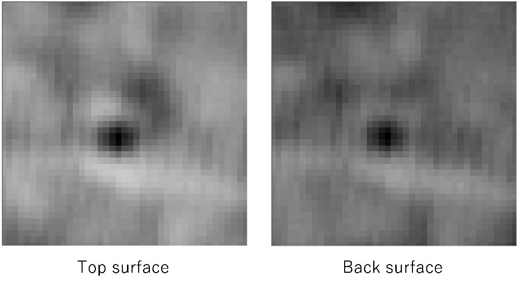
To create an artificial defect in a 3D-printed part, the researchers first fabricated an aluminum plate with a millimeter-scale hole drilled into it, and affixed on top of that a thin, defect-free aluminum plate. They then scanned a laser across the surface and detected the resulting ultrasonic vibrations from the aluminum. Mathematical processing of these vibrations enabled a graphical readout that highlighted the location and size of the internal defects.
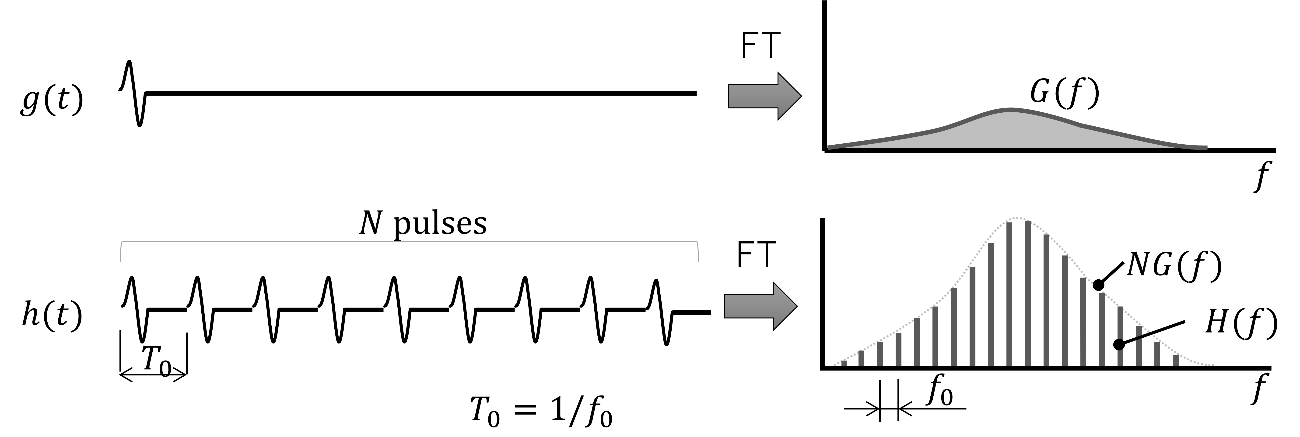
"We systematically varied the laser pulse duration, frequency range, and repetition frequency to optimize imaging of defects, and developed a theoretical analysis of our findings," says Takahiro Hayashi. "Advanced tests on a 3D-printed alloy commonly used as a benchmark in research indicated that we can even detect defects that are only 500 micrometers in size."
These results have diverse applications. By further optimizing the defect detection system, one could detect damage to a 3D-printed part as fabrication proceeds, and thus repair it in real time with the same ease as is done in machining. In so doing, the Osaka University researchers are enhancing the practicality of 3D printing for building intricate devices on a commercial scale.

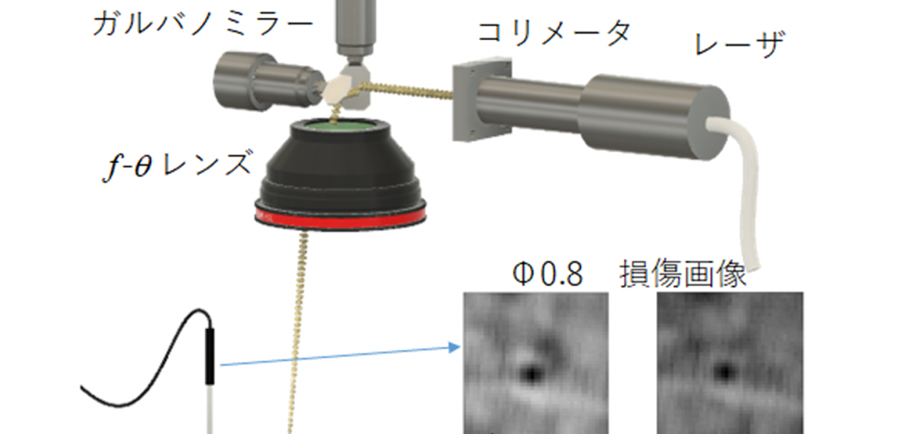
Fig.1 Experimental configuration (credit: Non-contact imaging of subsurface defects using a scanning laser source, T. Hayashi, N. Mori, and T. Ueno, Ultrasonics 2021)

Fig.2 Fourier transforms of the pulse wave and periodic pulse train (credit: Non-contact imaging of subsurface defects using a scanning laser source, T. Hayashi, N. Mori, and T. Ueno, Ultrasonics 2021)

Fig.3 Images of the 0.8-mm-diameter defect using waveforms detected on the top and back surfaces (credit: Non-contact imaging of subsurface defects using a scanning laser source, T. Hayashi, N. Mori, and T. Ueno, Ultrasonics 2021)
The article, "Non-contact imaging of subsurface defects using a scanning laser source," was published in Ultrasonics at DOI: https://doi.org/10.1016/j.ultras.2021.106560
