
Dominant factor of carrier transport mechanism in multilayer graphene nanoribbons revealed
A research team led by Osaka University precisely set the number of layers in multilayer graphene nanoribbons, controlling the semiconducting and metallic properties of filed effect transistors and establishing a design guideline for the practical applications of graphene devices
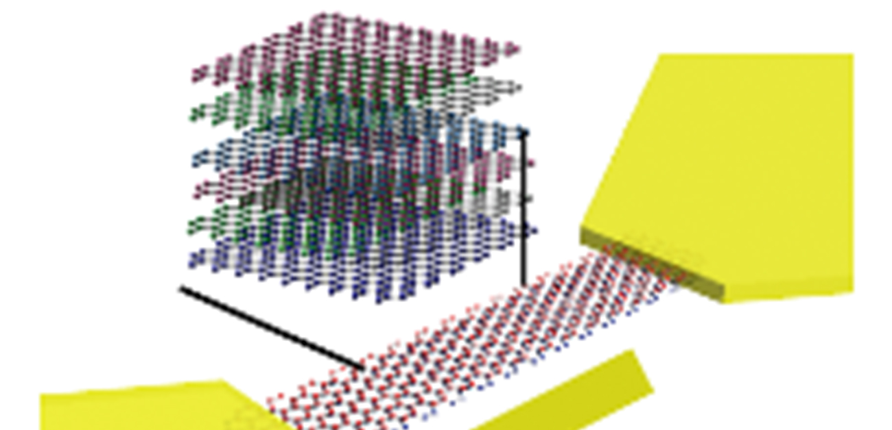
Researchers from Osaka University, Toyo University, and Kyushu Institute of Technology clarified the expression mechanism of semiconducting and metallic properties in graphene nanoribbons (GNRs) by analyzing the carrier transport properties in the field effect transistor (FET) with a multilayer GNR channel (Fig. 1).
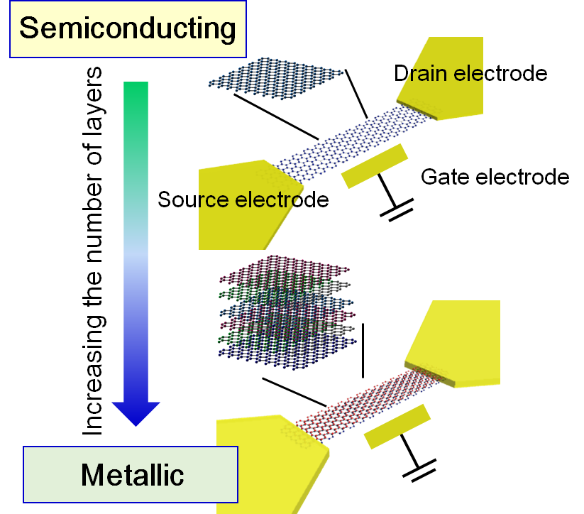
Fig. 1 Carrier transport characteristics of the FETs using the GNR channel
The research team fabricated multilayer GNRs with precisely controlled numbers of layers via a chemical vapor deposition method using a solid template. “This enabled us to compare the observed carrier transport properties in the FET using a multilayer GNR channel with various numbers of layers and device simulations based on theoretical calculations,” explains first author Ryota Negishi.
The study shows that the carrier transport behavior of the FET-GNR changes from semiconducting to metallic properties as the effect of the charged impurities on the device substrate (SiO2/Si) is reduced, namely semiconducting behavior for few layers (1-3 layers) and metallic behavior for multilayers (6-8 layers) as shown in Fig. 2.
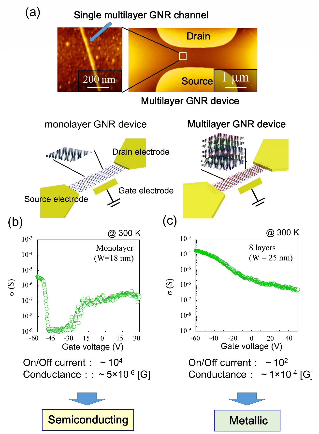
Fig. 2 (a) Field effect transistor using a single multilayer GNR channel. Transfer characteristics of (b) monolayer GNR device and (c) multilayer GNR device.
Fig 3(a) and 3(b) show the surface potential map of the monolayer and multilayer graphene calculated by the device simulation. In the case of monolayer GNR, the local high potential barriers are formed by the charged impurities on the substrate; however, in the case of multilayer GNRs, the surface potential becomes flat due to the field screening effect between layers.
Fig 3(c) and 3(d) schematically show the surface potential of monolayer and multilayer GNRs, respectively. The carrier transport of the monolayer GNR on the device substrate is affected by the local high potential barriers due to the charged impurities and hence shows hopping conduction over the barriers assisted by thermal energy. In particular, in a thin one-dimensional structure such as a monolayer GNR, the conduction electrons are localized and exhibit semiconducting-like properties because the locally formed potential barriers divides the current pass of the thin GNR channel. On the other hand, in a multilayer GNR, the electric field of the charged impurities is dramatically reduced as the number of layers increases due to the screening effect between layers, and the potential near the top layer becomes flat and shows the metallic characteristics with high conductivity.
Fig 3(e) shows the observed carrier transport properties of the FET with GNR channel as a function of the number of layers. After the number of layers reaches around five, the carrier transport characteristics change from semiconducting to metallic properties. A film thickness of five layers is in good agreement with the screening length (~1.5 nm) of the electric field due to the charged impurities that exist on the substrate. This indicates that carrier transport characteristics (i.e. semiconducting and metallic properties) in actual GNR devices are decided by the presence or absence of environmental effects.
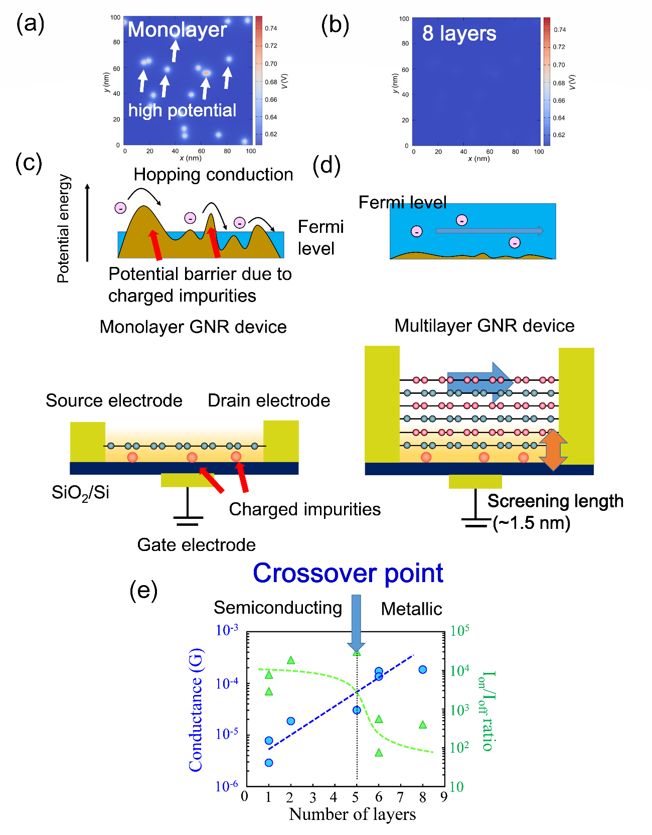
Fig. 3 Surface potential map of (a) monolayer and (b) eight layers using theoretical calculation, schematic drawings of potential in the cross section of (c) monolayer and (d) eight layers and carrier transport properties of the GNR as a function of number of layers
“We have succeeded in controlling semiconducting and metallic properties of FETs using multilayer GNRs by modulating the number of layers,” says Ryota Negishi. “GNRs with excellent carrier transport properties are attracting attention as next-generation electronic device materials. This study provides design guidelines for GNRs that incorporate actual device structures. This achievement is an important milestone that will accelerate the application of GNR materials for purposes such as high-speed transistors and ultra-thin wiring.”
The article, “Crossover point of the field effect transistor and interconnection applications in turbostratic multilayer graphene nanoribbon channel” was published in Scientific Reports at DOI: https://doi.org/10.1038/s41598-021-89709-z.