
Semiconductor spin transport devices with the highest performance and the lowest electric power
A group of researchers from Osaka University’s Graduate School of Engineering Sciences and SANKEN, and the Advanced Research Laboratories of Tokyo City University has developed a new technique in semiconductor (SC) spintronic devices using germanium (Ge), achieving the best device performance.
Ge, which has higher carrier mobility for both electrons and holes than silicon (Si), is gathering attention as a material for optoelectronic devices in the next generation. Researchers around the world are trying to create spin-electronic devices with non-volatile memory functionality in Ge-based optoelectronic devices through electrical injection into SCs in order to utilize the spin degree of freedom of conduction electrons.
In 2011, a group from the U.S. achieved electrical spin injection and transport in bulk n-type Ge using an Fe/MgO/n-Ge tunnel junction at low temperature. However, insulator tunnel barriers such as MgO cause a high parasitic resistance at the source and/or drain contacts, inducing a decrease in the MR ratio, the rate of change in resistance caused by the state of the magnetic field. A high voltage is necessary to detect spin injection and transport due to the presence of the MgO tunnel barrier layer, which exhibits high MR ratio. (Higher MR ratio makes it possible to obtain larger output signals.)
Since the insulator tunnel barrier highly affects the MR ratio, an important performance index in applications, it was difficult to achieve both highly efficient spin injection and low electric power at the electrodes in SC devices.
Using a technique to form Heusler alloy (a high performance spintronics material) on Ge at low temperatures and their unique doping technique, the researchers verified spin transport at room temperature.
This group also developed growth techniques for single-crystalline Co2FeAl0.5Si0.5 (CFAS) layers on Ge and Schottky-tunnel barrier electrodes with low values of the resistance area product (RA) for Ge spintronic devices. However, MR ratio was quite low (≤0.001%) at room temperature. It is required to obtain large spin signals at room temperature in order to realize a MOSFET (metal-oxide-semiconductor field-effect transistor) type of spin transistor, i.e., spin-MOSFET, which is expected to realize a nonvolatile memory function.
Their recent studies showed that the mutual diffusion (interdiffusion) of Ge and most notably Co from Co2FeAl0.5Si0.5 (CFAS) created an interface region of ∼5nm, which had a gradual decrease in the electrode spin polarization and ultimately affected the magnitude of the spin signal detected. (https://journals.aps.org/prb/abstract/10.1103/PhysRevB.98.115304)
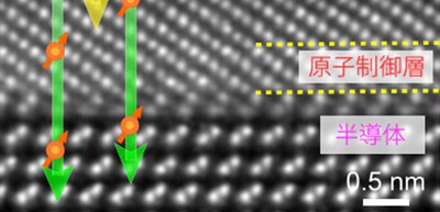
In this study, the researchers showed an efficient spin injection technique for a SC using an atomically controlled ferromagnet/ferromagnet/semiconductor heterostructure with low-resistive Schottky-tunnel barriers. They inserted iron (Fe) atomic layer at the Heusler/Ge, which limited the interdiffusion at the interface and increased MR ratio at room temperature.
They theoretically found that the CFAS/Fe5–6/Ge heterostructure had energy-band symmetry matching and led to efficient injection of spin-polarized electrons into the conduction band of Ge.
The room-temperature MR ratio for the lateral spin-valve (LSV) with Fe was ∼0.04%, which is approximately two orders of magnitude larger than those in the LSV devices without insertion of Fe atomic layers. The devices reduced the electric power for obtaining the largest MR ratio at room temperature down to ∼0.12 mW, one order of magnitude lower than that (∼1.15 mW) in Si-based LSV devices with MgO tunnel barriers.
This group achieved highly efficient spin injection at room temperature and low contact resistance in SC devices by using electrodes with contact resistance of several orders of magnitude less than the conventional one.
Their achievements will lead to the development of SC spintronics devices operable at room temperature, contributing to low power IoT (Internet of Things) and Artificial Intelligence (AI) technologies.
If highly efficient spin generation technology for achieving Ge-based spintronic devices is established, this group’s achievements will be a spintronics technology for innovating next-generation SC technologies in terms of low power consumption and high-speed operation.
Figure 1
Figure 2
The article, " Spin injection through energy-band symmetry matching with high spin polarization in atomically controlled ferromagnet/ferromagnet/semiconductor structures," was published in NPG Asia Materials at DOI: https://www.nature.com/articles/s41427-020-0228-5.
Related Links
Hamaya Laboratory, Graduate School of Engineering Science, Osaka University (link in Japanese)