A novel recipe for efficiently removing intrinsic defects from hard crystals
A team of researchers from Osaka University, the Institute for High Pressure Physics and the Institute for Nuclear Research of Russian Academy of Sciences (Russia), and TU Dresden (Germany), discovered an effective method for removing lattice defects from crystals. Their research results were published in Journal of Physics: Materials .
Boron, a semiconductor, has a variety of crystal structures, but all of them have large amounts of lattice defects that spoil the state of crystalline order. In this study, the team obtained an ordered phase of boron by adding hydrogen (hydrogenation) at high temperatures and through dehydrogenation by low-temperature annealing. This new method is the theoretical result by the research groups in Japan and Germany of a phenomenon that the Russian groups discovered in experiments.
Lattice defects present in all materials influence many of their electrical properties. The proper use of crystalline defects is useful in the electronic applications of semiconductors. The electrical conductivity of semiconductors can be enhanced by doping to produce n (negative)-type or p (positive)-type semiconductors. This control of lattice defects is called “valence electron control” and is achieved by placing dopants (impurities) into the atom sites. However, impurity atoms that occupy the interstitial sites are not useful in controlling valence electrons.
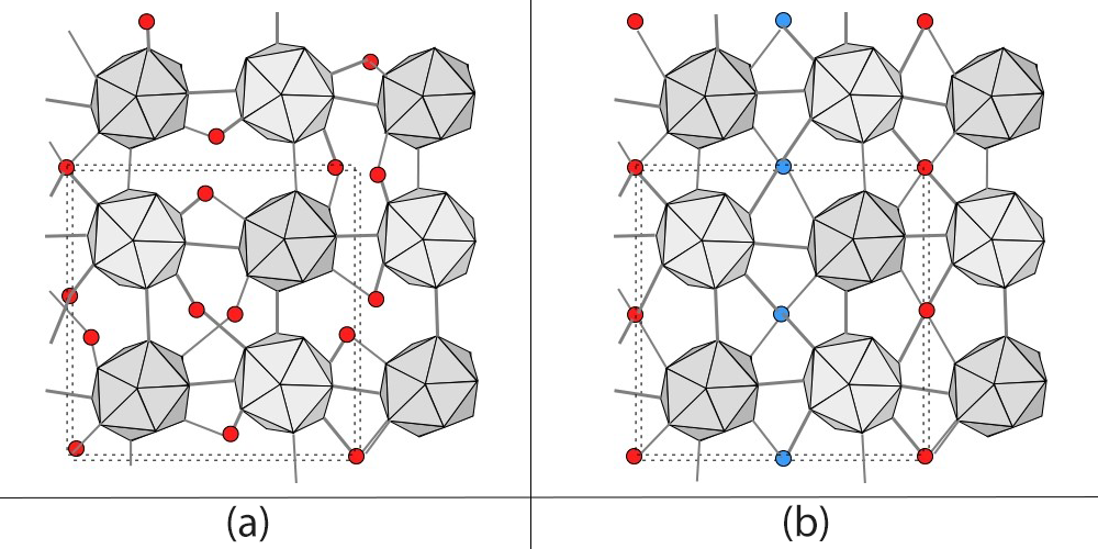
In a boron crystal, many atoms are randomly arranged in the interstitial sites (Figure 1 (a)). In addition, its crystal structure was too hard for the interstitial atoms to reach desirable sites. To render boron crystals as excellent semiconductor materials, it is necessary to rearrange randomly distributed boron atoms into an ordered structure.
Thus, this team created α-tetragonal (α-T) boron crystal at a high temperature and pressure, with a large amount of hydrogen as dopant. The obtained samples had a lot of defects. As shown in Figure 1 (a), while the B 12 icosahedral boron clusters (gray) are ordered, boron atoms (red) and hydrogen atoms in the interstitial sites are randomly arranged (hydrogen atoms are omitted in the figure). Later, when recovering the samples to ambient conditions and annealing them at moderate temperatures, the removal of hydrogen atoms and the ordering of interstitial boron atoms occurred simultaneously (Figure 1 (b)). This indicates that the random arrangement of interstitial atoms becomes an ordered structure. This is the first time an ordered boron crystal with a large unit cell (a unit cell containing more than 50 boron atoms) was obtained.
Generally, a crystal takes a more ordered structure at low temperatures. Usually, crystallization occurs at high temperatures, which induce many defects, and these defects are solidified at low temperatures. However, when volatile hydrogen atoms are incorporated beforehand, they are easily released by annealing. Upon hydration releases, the migration of atoms is induced, achieving the ordering of boron atoms. This transition is a kind of “cooperative phenomenon” between two different changes: diffusion of hydrogen and the ordering of host atoms.
Associate Prof. Shirai from Osaka University says, “In addition to boron, our method of removing defects can also be applied to carbon-based materials, such as fullerene, which are very hard and have a high melting point. Because removing defects from these hard materials is difficult, our recipe will be an efficient method of removing defects for other semiconductor materials as well.”

Figure 1.
(a) Normal structure of α-tetragonal boron. While icosahedra of boron (gray) have an ordered atomic arrangement, interstitial boron atoms (red) are randomly arranged. (b) Interstitial atoms are arranged in an ordered form in which the linear chains of interstitial atoms with different heights (red and blue) are alternately arranged.
The article, “Hydrogenation, dehydrogenation of α-tetragonal boron and its transition to δ-orthorhombic boron,” was published in the Journal of Physics: Materials at DOI: https://doi.org/10.1088/2515-7639/ab2c8d .
This research was funded by: The Innovative Professional Development project of Professional development Consortium for Computational Materials Scientists, The Research Program of Five-star Alliance in NJRC Mater. & Dev., The German Research Foundation (DFG) under grant number SE 651/45-1 and financial support by the Center for Advancing Electronics Dresden.
Related links
