
Non-contact measurement device developed for measuring charge carrier mobility
Accelerates the development of semiconductor devices!
A group of researchers at the Graduate School of Engineering Osaka University -- Dr. Yoshihito HONSHO (then Japan Society for the Promotion of Science fellow), Tomoyo MIYAKAI (2nd year in the first-term doctoral program), Dr. Tsuneaki SAKURAI (Japan Society for the Promotion of Science fellow), Assistant Professor Akinori SAEKI , and Professor Shu SEKI -- succeeded in developing a technique for measuring the charge carrier mobility at the insulator-semiconductor interface using an original non-contact microwave measurement device.
This technique enabled them to restrict the measurement to hole and charge carrier mobility at the insulator-semiconductor interface.
Wide employment of "field-induced time-resolved microwave conductivity" (FI-TRMC) technology will almost certainly enable more rapid development of high-performance FET devices, solar cells, and more.
Abstract
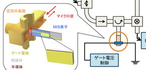
We have successfully designed the geometry of the microwave cavity and the thin metal electrode, achieving resonance of the microwave cavity with the metal-insulator-semiconductor (MIS) device structure. This very simple MIS device operates in the cavity, where charge carriers are injected quantitatively by an applied bias at the insulator-semiconductor interface. The local motion of the charge carriers was clearly probed through the applied external microwave field, also giving the quantitative responses to the injected charge carrier density and charge/discharge characteristics. By means of the present measurement system named field-induced time-resolved microwave conductivity (FI-TRMC), the pentacene thin film in the MIS device allowed the evaluation of the hole and electron mobility at the insulator-semiconductor interface of 6.3 and 0.34 cm2 V−1 s−1, respectively. This is the first report on the direct, intrinsic, non-contact measurement of charge carrier mobility at interfaces that has been fully experimentally verified.

Figure 1
To learn more about this research, please read the full research report entitled " Evaluation of Intrinsic Charge Carrier Transport at Insulator-Semiconductor Interfaces Probed by a Non-Contact Microwave-Based Technique " at this page of the Scientific Reports website.
Related link :