

Discovery of giant Rashba Effect at semiconductor-metal interface
Synopsis
Under the leadership of TAKAYAMA Akari , graduate student at the Graduate School of Science, Tohoku University, TAKAHASHI Takashi , Professor, Advanced Institute for Materials Research, Tohoku University, and OGUCHI Tamio , Professor, Institute of Scientific and Industrial Research, Osaka University , a team of researchers has succeeded in clarifying a central mechanism of an effect in the creation and control of the spin-flow in spintronic*1 devices. This effect, called the Rashba Effect*2, is observed at the semiconductor-metal interface. This mechanism has drawn attention as a pillar of next-generation spintronic devices. The Rashba effect was observed by examining spin*3 states of ultra-thin bismuth film with an ultrahigh resolution spin-resolved photoemission spectrometer. This discovery opens a path for the development of semiconductor electronic devices and next-generation spintronic devices using material interfaces.
The important findings of this team were published in the April 11th issue of the American Chemical Society magazine, Nano Letters .
Background
Along with the popularization of smaller, faster, and more energy-efficient electronic information devices, researchers are engaged in active development of devices referred to as "spintronics" that make use of the new technology. Spintronics technology makes use of the magnetic properties of the spin of electrons. In spintronics, electron spin is handled in terms of binary digital information, either 1 or 0. As electrons can flow without electrical resistance and electronic spin does not generate heat in their transmission and control, power requirements can be drastically reduced. However, to realize such spintronic devices, materials used as key components must be developed. As a storage device, Magnetoresistive Random Access Memory (MRAM)* based on ferromagnetic metal with magnetic memory elements is already in practical use and expectations for computers with less power consumption are high.
On the other hand, conventional semiconductor devices have no magnetic properties, so they cannot align spin directions with electronic signals. However, recent research has clarified that there is a "Rashba effect" which changes spin direction on the surface of heavy metals in a semiconductor interface.
The Rashba effect is a relativistic effect called "spin-orbit interaction"*5, determining spin direction. The use of the Rashba effect will lead to higher speed and higher integration of spintronics devices. (Figure 1)
Rashba effect has great possibilities; however, there have been large challenges in developing devices using this effect. One challenge was that the relativistic effect was weak at the semiconductor interface in devices, thereby also reducing the Rashba effect. The other challenge was that experimental observation of electrons at the interface was so difficult that the Rashba effect had not been fully understood. In order to develop high-speed and energy-saving spintronic devices, these obstacles needed to be overcome.
Findings
In this research, the joint research group of Tohoku University and Osaka University set out to determine the state of electron spin of bismuth (Bi) metal film using a spin-resolved photoemission spectrometer*6. (Figure 2) The group created a thin Bi film on the surface of a silicon (Si) semiconductor and conducted experiments using a spin-resolved photoemission spectrometer developed by Tohoku University. (Figure 3)
The heavy metal Bi showed a strong Rashba effect on the surface and electrons showed a large spin polarization perpendicular to the direction of motion. This group determined for the first time in the world that the spin polarization of the surface electrons changes in relation to the relative thickness (or thinness) of the film. (Figure 4)
Furthermore, the group found that the electron energy state varies in accordance with the film thickness. As a result of theoretical analysis on the Bi/Si surface (at the Bi/Si interface) they discovered a Rashba effect that had the opposite spin direction from the Bi surface. (Figure 5) They also found that the size of the effect was significantly larger than the effect at the conventional semiconductor interface.
Future development
This research has experimentally indicated that the electron spin state between metal and semiconductor that had been difficult to observe had the same structure as the electron spin state on the surface. Furthermore, they also concluded that the Rashba effect observed at the interface between Bi and Si was significantly larger than the Rashba effect at the semiconductor interface and that it is possible to control the spin accurately with less electric power. Therefore, this finding will make possible more effective energy-saving and highly accurate spintronic devices. It is expected that the development of new spintronic devices making use of this giant Rashba effect at the metal-semiconductor interface will be greatly enhanced.
This achievement was obtained through Grants-in-Aid for Scientific Research (S) supported by the Japan Society for the Promotion of Science, " Electronic states of novel functional materials studied by ultrahigh-resolution three-dimensional spin- and angle-resolved photoemission spectroscopy ."(project leader: TAKAHASHI Takashi)

Figure 1
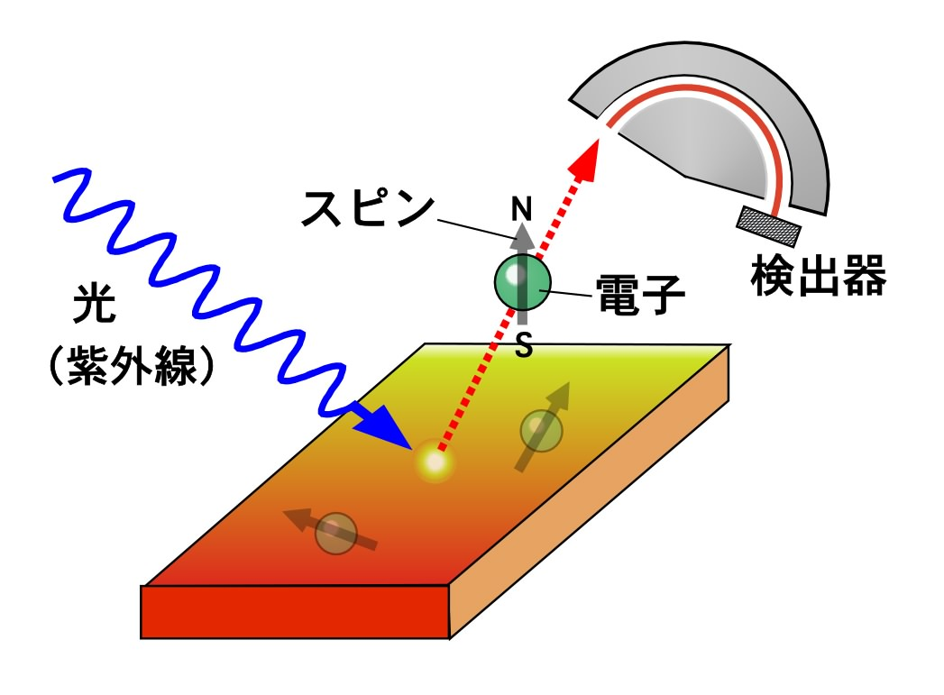
Figure 2
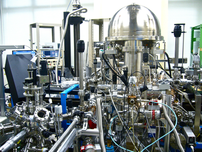
Figure 3
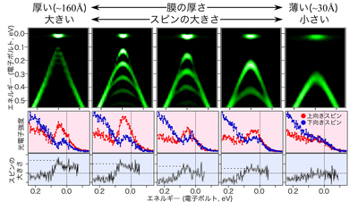
Figure 4
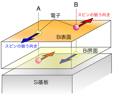
Figure 5
Notes
- Spintronics -- is a research field in the development of new electronic devices (transistors and diodes) that makes use of electron magnetic properties. In spintronics, signals are processed by replacing the 'spin up' and 'spin down' states with the electrical signals '1' and '0'. Electronic spin responds quickly and generates less thermal energy. Spintronics devices using electronic spin is considered a major candidate for next-generation electronic devices with ultra-high speed and ultra-low power consumption.
- Rashba effect -- is a phenomenon observed on a two-dimensional plane. Electrons affected by this effect will have a spin direction perpendicular to the 2D plane of electron motion. (Figure 1) In a normal Rashba effect, the number of up spins and down spins is the same so the total amount spins' angular momentum is zero. When applying an electric field, however, the number of electrons with spins facing a specific direction increases and spin current flows. If we can clarify such spin behavior and control the spin, it will lead to the discovery of new quantum phenomena and increased development of spintronic devices. Placing great hopes on such, researchers are vigorously pursuing further research.
- Spin -- is the orbital angular momentum of the electron, giving the electron a magnetic property. There are two states; either up or down on the axis of rotation. This spin axis faces a various directions through electromagnetic interaction in materials. In ordinary metals and semiconductors, the number of electrons with up spin and down spin is the same. Therefore, magnetism is zero. However, in ferromagnetic substances, the number of electrons with spin facing only one direction increases, generating strong magnetism.
- Magnetoresistive Random Access Memory (MRAM) -- is a new technology that makes use of electron spin as a memory element. Computer information is stored in the spin's magnetized state. In MRAM, the electrical resistance of an element is changed by controlling its spin direction. This high or low electrical resistance is handled in terms of binary digital information, either 1 or 0. In MRAM electron spin provides non-volatile memory, therefore information is retained when power is turned off. For this reason, standby power consumption can be drastically reduced and energy saved.
- Spin orbit interaction -- is the momentum between the spin of the electron and the angular momentum of its orbit and is derived from a relativistic effect. The electron has an electrical charge. Therefore, when it moves around the nucleus, electricity flows and a magnetic field is generated. At the same time, as the electron also has spin, there is an interaction between the magnetic property of spin up and spin down (electron's intrinsic spin) and the magnetic field caused by orbit motion (electron's orbital motion). The spin orbit interaction is present in all materials, but stronger effects are shown especially in heavy atoms. For the next-generation spintronics, the development of technology using this spin orbit interaction is expected.
- Spin-resolved photoemission spectroscopy -- is an analytical technique (employing a spectroscope or spectrometer) for measuring energy, momentum, and spin of electrons through external photoelectric effects released from surfaces of crystals irradiated by high-intensity UV. (Figure 2) This method enables researchers to determine how the direction and size of electronic spin influence energy and momentum of the electron. Formerly, the efficiency of spin detection was so low that it was difficult to determine the electron spin state with very high accuracy. After making numerous improvements, Tohoku University succeeded in developing a three-dimensional spin- and angle-resolved photoemission spectroscope (ARPES) with the highest resolution in the world.