
Spin transport in germanium-based electronic devices at room temperatures demonstrated
A step toward next-generation semiconductor devices
Since germanium (Ge) has approximately twice the mobility for electrons and four times the mobility for holes than does silicon (Si), it is anticipated as a next-generation semiconductor channel material, an alternative to Si. In the most advanced semiconductor research, core semiconductor technology, Ge-CMOS (complementary metal–oxide–semiconductor), is being developed. Furthermore, spintronics research on adding nonvolatile memory functionality through spin injection into Ge is also being performed all over the world.
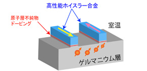
A joint group of researchers led by Professor HAMAYA Kohei at the Graduate School of Engineering Science, Osaka University, and Professor SAWANO Kentaro at Tokyo City University, demonstrated spin transport in Ge-based micro devices. This group achieved this through the use of Ge-based spintronics devices with their own spin injection/detection technique in which high-quality spintronics material (Heusler alloy) and impurity doping on the Ge atomic layer were used in combination.
The group led by Professor Hamaya had previously succeeded in fabricating ferromagnetic Heusler alloy on the Ge (111) layer and achieving generation, manipulation, and detection of pure spin currents at room temperatures by using an atomic layer doping technique developed by the group led by Professor Sawano in combination.
The group designed a device in consideration of relation between spin scattering and impurity doping levels in Ge, demonstrating spin transport in Ge-based electronic device structure at room temperatures, a world first. The group also experimentally clarified that the spin diffusion length in densely doped Ge at room temperature was approximately 0.5μm.
Ge is anticipated as a next-generation core semiconductor channel material. The establishment of spintronics, a revolutionary technique to add nonvolatile memory functionality into Ge, will realize semiconductors with high speed operations and low energy consumption. Resistance of the device structure developed by this group is lower than that of conventional tunnel barrier layer-type devices, so it is hoped that low-voltage-driven devices with that structure will be demonstrated as well.
Abstract
We demonstrate electrical spin injection and detection in n-type Ge (n-Ge) at room temperature using four-terminal nonlocal spin-valve and Hanle-effect measurements in lateral spin-valve (LSV) devices with Heusler-alloy Schottky tunnel contacts. The spin diffusion length (λ Ge ) of the Ge layer used (n ~ 1 × 10 19 cm −3 ) at 296 K is estimated to be ~0.44 ± 0.02 µm. Room-temperature spin signals can be observed reproducibly in the low bias voltage range (≤0.7 V) for LSVs with relatively low resistance–area product (RA) values (≤1 kΩ µm 2 ). This means that the Schottky tunnel contacts used here are more suitable than ferromagnet/MgO tunnel contacts (RA ≥ 100 kΩ µm 2 ) for developing Ge spintronic applications.
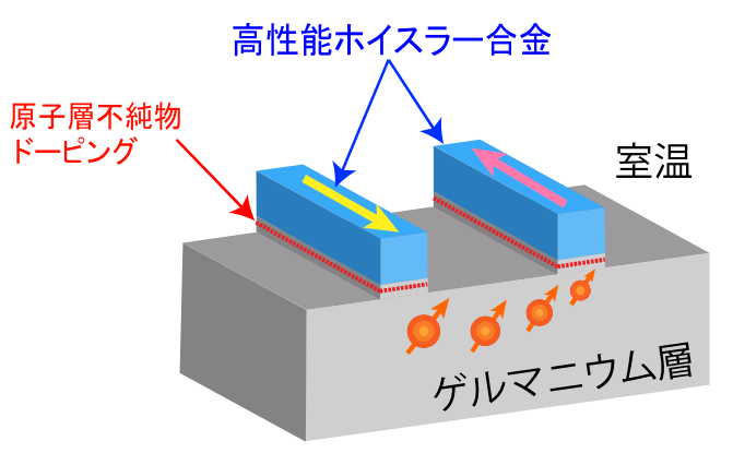
Figure 1
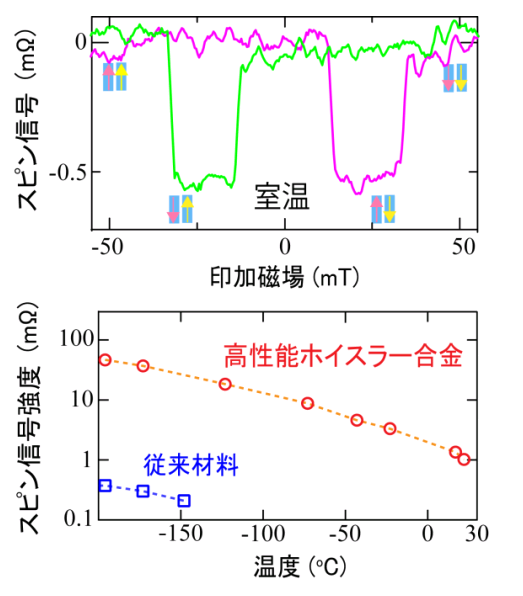
Figure 2
To learn more about this research, please view the full research report entitled “ Spin Transport and Relaxation up to 250 K in Heavily Doped n-Type Ge Detected Using Co2FeAl0.5Si0.5 Electrodes ” at this page of the Applied Physics Express website.
Related link