
Development of technology for increasing by 10 times the manufacturing speed of next-generation semiconductors
a great step in the realization of EUV lithography
Under the leadership of TAGAWA Seiichi , Visiting Professor and OSHIMA Akihiro , Visiting Associate Professor, Institute of Scientific and Industrial Research, Osaka University, a group of researchers developed technology capable of increasing advanced semiconductor wafer throughput by a factor of 10 or greater in comparison with conventional technology.
Extreme-ultraviolet (EUV) lithography costing as much as 10 billion yen is, despite its cost, considered a major player in lithography technology in the manufacturing of next-generation semiconductor devices. However, low wafer throughput (less than one tenth of the goal) due to the low power source for EUV lithography has been the major problem.
Based on on the standard reaction theory, this group standardized the sensitivity of the resist. However, the sensitivity of the resist is approaching its physical limit and the throughput goal is not attainable with low exposure sources. The development of an adequate exposure source has been a stumbling block in introducing EUV lithography into semiconductor mass production.
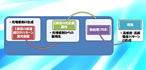
This group thoroughly reviewed both the exposure process and photosensitivity of the resin [resist] and succeeded in developing revolutionary technology for achieving the desired throughput by simultaneously increasing resist sensitivity in conjunction with exposure to a low EUV power source. This group's achievement will help make the long-awaited EUV lithography a practical reality.


Related link