About this research

IE Yutaka
- SANKEN (The Institute of Scientific and Industrial Research)
- Professor

Breaking conventional wisdom: A new material improves the performance of organic photovoltaic cells
A significant step toward the commercialization of low-cost, large-area organic photovoltaic cells
- Core-to-core overlapping between the central regions of polymer backbones enables charge carrier mobility an order of magnitude higher than conventional values, even in low-crystallinity polymer semiconductors where the chains are not well ordered.
- This work resolves the trade-off in polymer semiconductors between solubility and charge transport, where improving solubility typically reduces electrical conductivity, while enhancing charge transport often compromises solubility.
- Achieved world-leading power conversion efficiency in organic photovoltaic (OPV) cells using a low-cost fullerene-based material.
Outline
A collaborative research team including Professor Itaru Osaka and Assistant Professor Tsubasa Mikie of the Graduate School of Advanced Science and Engineering, Hiroshima University; Professor Hideo Ohkita of the Graduate School of Engineering, Kyoto University; and Dr. Yusuke Nishiyama of JEOL Ltd. has elucidated the origin of the high charge carrier mobility of PTNT2T, a polymer semiconductor previously developed by the Hiroshima University group. The team also achieved a power conversion efficiency among the highest ever reported worldwide for organic photovoltaic (OPV) cells.
Until now, it has been thought that, in polymer semiconductors, forming a well-ordered crystalline structure in which the polymer backbones are regularly aligned is essential to enhance charge transport properties. However, previous study has shown that PTNT2T exhibits high charge transport performance despite its low degree of crystalline order (crystallinity). In this study, the research team discovered that efficient charge transport pathways are formed through core-to-core overlapping, in which the TNT cores that make up the polymer backbones overlap at the molecular level, enabling high charge transport despite its low crystalline order. Furthermore, the team demonstrated that OPVs employing PTNT2T as the donor material in the photoactive layer can maintain a high fill factor (FF) even in thick photoactive layers. In particular, OPVs using a fullerene derivative (PCBM) as the acceptor material achieved a fill factor exceeding 80% in active layers thicker than 300 nm for the first time in the world, while also delivering a world-record power conversion efficiency of 12%. Since large-area fabrication of OPVs requires thick photoactive layers from manufacturing standpoints, the ability to maintain device performance at greater active-layer thicknesses is critically important. The ability to achieve high power conversion efficiency using PCBM, a relatively inexpensive acceptor material, is also significant for reducing the cost of OPV devices.
These findings provide a new design strategy for developing high-mobility polymer semiconductors that do not rely on high crystallinity and are expected to accelerate the commercialization of organic photovoltaic (OPV) technologies, which have attracted increasing attention in recent years as next-generation solar cells.
Research Background
Polymer semiconductors are semiconductor materials that can be easily processed into thin films using solution-based coating techniques. They are expected to find widespread application in organic electronic devices such as organic transistors and organic photovoltaic (OPV) cells. The development of polymer semiconductors with high charge carrier mobility is therefore a key challenge for improving the performance of these devices.
Until now, it has been believed that enhancing the degree of ordering (crystallinity) between polymer backbones is crucial for improving charge-carrier mobility in polymer semiconductors. On the other hand, there has been a trade-off whereby enhancing crystallinity to improve charge carrier mobility reduces solubility in solvents, making it difficult to fabricate thin films using solution-based coating processes. In addition, in OPVs, the low charge carrier mobility of polymer semiconductors has been a longstanding issue, as device performance declines significantly when the thickness of the photoactive layer exceeds 100 nm. However, for the fabrication of large-area modules, a photoactive layer thickness of at least 300 nm is required to ensure uniform film formation over a large area. Therefore, the development of polymer semiconductors that combine excellent charge transport properties with high solubility has been a critical challenge for the commercialization of OPVs.
Research Contents
In this study, the research team focused on the polymer semiconductor PTNT2T (Fig. 1), which was previously developed by a group at Hiroshima University. PTNT2T had been found to possess an interesting combination of properties: unlike conventional polymer semiconductors, it shows high charge carrier mobility despite its low crystallinity and high solubility. To deeply understand charge transport mechanism in the polymer, the researchers conducted a detailed investigation and explored its application in organic photovoltaic (OPV) devices.
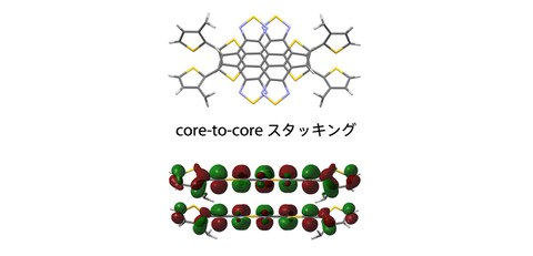
First, analyses based on the orientation of the polymer backbone inferred from variable-angle spectroscopic ellipsometry (VASE) by Team Director Keisuke Tajima and Senior Scientist Kyohei Nakano at RIKEN, together with the effective mass along the backbone direction predicted by quantum chemical calculations performed by Professor Hiroyuki Ishii of the University of Tsukuba, revealed that PTNT2T achieves high charge carrier mobility despite its low crystallinity because charge transport is highly efficient along the polymer backbone. On the other hand, a more detailed analysis of the aggregate structure of PTNT2T revealed a strong interaction between polymer backbones. Solid-state NMR measurements performed by Dr. Yusuke Nishiyama of JEOL Ltd., together with crystal structure analysis of model compounds, revealed that PTNT2T forms a core-to-core overlapping structure in which the TNT units constituting the polymer backbone exhibit extensive overlap (Fig. 2). Furthermore, quantum chemical calculations performed by Professor Yutaka Ie of the Institute of Scientific and Industrial Research, the University of Osaka, revealed that this core-to-core overlapping increases the overlap of π electrons to approximately three times that found in conventional polymer semiconductors. These results demonstrated that PTNT2T is highly favorable for charge transport between polymer backbones. These findings indicate that PTNT2T achieves high charge carrier mobility despite its low crystallinity because efficient charge transport pathways are formed not only along the polymer backbone but also between polymer backbones through this unique molecular-level interaction. Electrical analyses conducted by a research group including Professor Hideo Ohkita at Kyoto University also revealed that charge recombination was significantly suppressed relative to charge collection.
Accordingly, the research team fabricated OPV devices using PTNT2T as the donor material in the photoactive layer. Notably, when PCBM was employed as the acceptor material, the devices exhibited an exceptionally high fill factor (FF) exceeding 80%, even with a photoactive layer thicker than 300 nm, approximately three times thicker than conventional devices. Furthermore, despite the thick photoactive layer, the power conversion efficiency reached 12%, which is among the highest reported in the world for devices of this type. In addition, even when a non-fullerene acceptor was used as an accepter material, the devices achieved a high power conversion efficiency (PCE) of 15.6%.
Fig. 1 Chemical structure of PTNT2T, a polymer semiconductor containing the TNT core (highlighted in red) previously developed by a research group at Hiroshima University. "Enhanced charge carrier mobility in a polymer semiconductor through structural extension" Press Release, November 18, 2024
Credit: IE Yutaka
Fig. 2 Crystal structure of a model compound of PTNT2T. Molecular orbitals are overlaid on the structure viewed from above (top) and from the side (bottom).
An extensive core-to-core overlapping formed, in which the TNT cores extensively overlap with one another.
This structure increases the overlap of the molecular orbitals to approximately three times that of conventional structures, enabling efficient charge transport between molecules.
Credit: IE Yutaka
Future Development
This study demonstrates that high charge transport can be achieved without enhancing crystallinity, overturning conventional principle in the field of polymer semiconductors. This breakthrough is expected to overcome the trade-off between high solubility and high charge carrier mobility, accelerating the development of high-performance and commercial polymer semiconductors. Furthermore, the ability to achieve high power conversion efficiency using the inexpensive acceptor material PCBM and a thick photoactive layer of 300 nm indicates a major step forward toward the commercialization and widespread adoption of OPVs.
Notes
The article, “Core-to-Core Overlap Promotes Interchain Charge Transport across Crystalline and Amorphous Regions in a Conjugated Polymer: High Fill Factors in Thick Organic Photovoltaic Cells,” was published in Chemical Science at DOI: https://doi.org/10.1039/d6sc01947a.