About this research

CHEN Chuantong
- SANKEN (The Institute of Scientific and Industrial Research)
- Specially Appointed Professor (Full-time)

High-strength Cu sintered bonding formed in air!
New technology for next-generation power semiconductors
- Researchers have developed a new technology that enables rapid, oxide-free bonding in air using copper paste sintering. Copper is regarded as a promising bonding material for next-generation power semiconductors because of its high thermal and electrical conductivity.
- Conventional Cu sintered bonding processes require a protective atmosphere, such as nitrogen gas, to prevent oxidation of copper caused by exposure to air. By developing a proprietary solvent, the researchers succeeded in suppressing oxidation of Cu particles and enabling sintered bonding even in air.
- The technology is expected to be applied to high-heat-dissipation, high-reliability bonding structures for next-generation power semiconductor modules and advanced semiconductors used in AI data centers. It may also contribute to cost reduction and energy efficiency through the simplification of production processes.
Outlines
A research group including Specially Appointed Researcher Fupeng Huo and Specially Appointed Professor Chuantong Chen of the Flexible 3D System Integration Laboratory of SANKEN, the University of Osaka, has developed a new technology that achieves high-strength sintered bonding while suppressing the oxidation of copper particles in air.
Copper (Cu) is attracting considerable attention as a bonding material for next-generation power semiconductors and high-performance electronic devices because it offers high thermal and electrical conductivity at a lower cost than silver (Ag). However, because copper is easily oxidized at high temperatures, conventional sintered bonding processes require operation in specialized environments using nitrogen gas or other protective atmospheres. This requirement has posed significant challenges in terms of production costs and equipment burden.
In this study, the research group developed a technology for controlling the oxidation and reduction of copper during the sintering process. Using a specially designed reducing solvent, the researchers successfully not only suppressed oxidation on the surface of copper particles but also removed oxygen from the copper oxide formed during the process, converting it back into metallic copper. Furthermore, the bonding produced through the sintering process exhibited superior strength as well as excellent thermal and electrical conductivity, confirming their reliability at a practical level.
This technology is expected to find applications in advanced electronic devices that require high heat dissipation and reliability, including wide-bandgap power semiconductor modules based on silicon carbide (SiC) and gallium nitride (GaN) for use in electric vehicles and power equipment, as well as AI data centers, high-performance computing systems, electric vehicles, and renewable energy systems. In addition, by simplifying the production process, the technology is expected to contribute to energy efficiency and reduced production costs, thereby playing a significant role in advancing next-generation semiconductor packaging technologies.
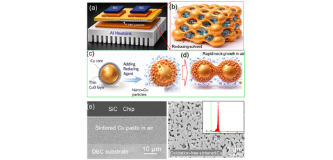
Fig. 1
(a) Cu sintered bonding structure in a SiC power module
(b) Schematic illustration of the sintered copper bonding layer developed in this study
(c)(d) Mechanism of copper oxidation suppression and rapid sintering in air
(e)(f) Cross-sectional observation of the bonding after sintering at 250°C for 5 minutes
Credit: CHEN Chuantong
Research Background
In the field of power electronics, there is a growing demand for power converters used in electric vehicles, renewable energy systems, and data centers to become smaller, higher performance, and more energy efficient. To achieve this, technologies for bonding components such as semiconductor chips to substrates and other materials are also essential. Bonding materials are required to provide high heat resistance and reliability. However, conventional lead-free solder, which has been the dominant bonding material, may not withstand the high-temperature operating environments of next-generation power semiconductors. As a result, active research and development efforts have been underway to develop new bonding materials.
For example, sinter bonding technologies using silver particles have attracted attention as promising alternatives. However, their practical implementation has been hindered by cost and technical challenges. In this regard, copper particles offer a cost advantage over silver particles and are also less susceptible to failure in environments carrying high electrical currents.
However, copper is easily oxidized, and the resulting copper oxide inhibits the sintering reaction. Consequently, bonding processes using copper are generally carried out either under protective atmospheres, such as nitrogen or anti-oxidation gases, or in vacuum environments to prevent oxidation. The additional costs and equipment required to maintain such atmospheres remain major obstacles. As a result, there is a need for copper pastes that exhibit oxidation resistance in air and facilitate the efficient formation of sintered joint structures.
Research Contents
The researchers developed a technology in which a specially designed reducing solvent converts the copper oxide layers (Cu₂O and CuO) formed on copper particle surfaces into copper nanoparticles smaller than 10 nm in diameter at room temperature. (1 nanometer = one billionth of a meter).
Specifically, the researchers developed a copper paste containing copper nanoparticles generated from the naturally formed oxide layer on the surface of copper particles by using a mixed solvent (consisting of a primary solvent and a co-solvent) that exhibits reducing properties at room temperature. They then evaluated its sintering performance.
As a result, under air atmosphere conditions, the researchers achieved a high bonding strength of 38.1 MPa in the bonding of a SiC chip to a DBC substrate through sintering at 250°C for just 5 minutes. Furthermore, the researchers successfully realized a rapid, oxidation-free copper sinter-bonding technology in air without the need for special protective atmospheres or vacuum equipment.
This reducing solvent remains within the bonded structure even after sintering and continues to provide anti-oxidation protection, thereby contributing to the long-term reliability of copper bonding. The researchers confirmed that the joint produced by sintering exhibited high strength and excellent thermal and electrical conductivity, demonstrating reliability at a practical level.
Social Impacts
The developed technology realizes high-strength sintered copper bonding in air, and is expected to contribute to reducing manufacturing costs, improving energy efficiency, and enhancing the reliability of electronic devices. In particular, through its application to next-generation power semiconductor modules, this technology is expected to improve the efficiency of electric vehicles and renewable energy systems, thereby contributing to the realization of a carbon-neutral society.
Notes
The article, “Oxidation-resistant and rapid Cu sintering in an air atmosphere via the synergistic strategy of sustained release reduction and in-situ surface nanostructuring,” was published in Chinese scientific journal of Journal of Materials Science & Technology at DOI: 10.1016/j.jmst.2026.05.041.