Advanced measurement technology for future semiconductor devices
Terahertz time domain spectroscopy for ultra-high frequency response of gallium oxide
1. Key points of the work
• An emerging semiconductor for future power devices, beta-gallium oxide (β-Ga2O3), was investigated using a technique called transmission terahertz time-domain spectroscopy (THz-TDS) for the first time
• The findings on the fundamental properties of β-Ga2O3 at THz frequencies are significant to the development of this semiconductor’s power electronic applications
• THz-TDS can be used as a noninvasive tool for the evaluation of electrical properties instead of conventional electrical measurements that degrade the semiconductor quality
2. Overview of the work
The β-Ga2O3 ultra-wide bandgap (UWBG) semiconductor [1,2] could revolutionize the power electronics industry with its superior material properties for efficient power conversion in comparison to current commercial semiconductors such as silicon carbide and gallium nitride (Figure 1). To develop electronic applications, material properties in the millimeter and terahertz wave regions must be elucidated. A research group including Associate Professor Makoto Nakajima, Verdad C. Agulto, Valynn Katrine Mag-usara of Osaka University, Toshiyuki Iwamoto of Nippo Precision Co., Ltd., Professor Yoshinao Kumagai, Associate Professor Hisashi Murakami, and Assistant Professor Ken Goto of Tokyo University of Agriculture and Technology employed a noninvasive technique called terahertz time-domain spectroscopy (THz-TDS) [3] to investigate β-Ga2O3 materials using THz waves [4] and demonstrated the viability of this tool for the practical evaluation of β-Ga2O3-based devices.
THz-TDS is used to measure the permittivity of a material – a fundamental property that describes how much electrical energy the material can store and is an important parameter relevant to power devices. The researchers determined the permittivity of β-Ga2O3 in the THz region using the THz-TDS technique. From the permittivity, they were also able to extract the electrical properties such as carrier density and resistivity with an accuracy that is comparable to conventional albeit invasive measurement methods used in the semiconductor industry. The researchers believe that the application of THz-TDS in semiconductor characterization would be advantageous towards the rapid development of β-Ga2O3 materials for future power devices.
The article, “Anisotropic complex refractive index of β-Ga2O3 bulk and epilayer evaluated by terahertz time-domain spectroscopy,” was published online in Applied Physics Letters on January 25, 2021, 11:00 AM Eastern Standard Time (January 26, 2021, 1:00 AM Japan Standard Time) at DOI: https://doi.org/10.1063/5.0031531.
3. Details of the work
Terahertz frequencies (about 100 GHz to 10 THz) lie between the microwave and infrared regions of the electromagnetic spectrum, with the frequency band around 100 GHz being considered as an ultra-high frequency region for the next-generation communication band also known as Beyond 5G/6G. By studying the interaction of semiconductors with THz radiation, various information about the semiconductor properties can be acquired. The THz-TDS investigation of β-Ga2O3 materials - semi-insulating bulk crystal and doped homoepitaxial film - was led by Associate Professor Makoto Nakajima of the Institute of Laser Engineering, Osaka University. The transmission of THz beam through the β-Ga2O3 materials was measured using the equipment developed by Nippo Precision Co. Ltd. (PNP) called Tera Prospector [5]. Since β-Ga2O3 is an anisotropic crystal (i.e., its properties vary along different crystal axes), the transmission measurements were done along two different crystal directions that are parallel to the a and b crystal axes. By evaluating the measured transmission, fundamental material properties such as the anisotropic complex refractive index [6] in the THz region were determined. The complex refractive index is in turn related to the material’s permittivity.
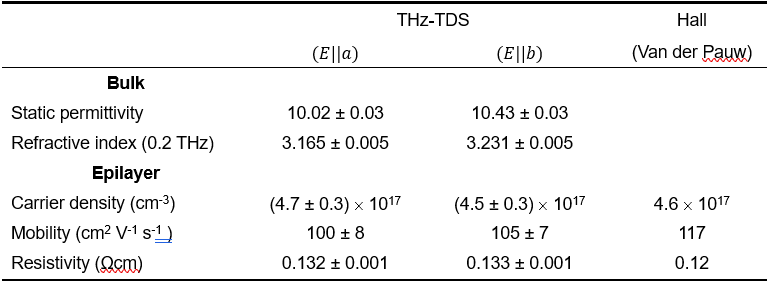
Using the THz-TDS technique, the researchers succeeded in obtaining the complex refractive index spectra in the terahertz band which is an ultra-high frequency region. Figure 2 shows the complex refractive index of the semi-insulating bulk crystal and the doped homoepitaxial film (or epilayer) in the THz region measured by THz-TDS. The semi-insulating β-Ga2O3 single crystal sample exhibits increasing refractive index with increasing frequency, which indicates the presence of phonon absorption in the infrared region. On the other hand, the n-type β-Ga2O3 epitaxial film exhibits increasing refractive index with decreasing frequency which is different from the semi-insulating sample. This increase in refractive index in the low-frequency side indicates absorption depending on the amount of carrier density in β-Ga2O3. By evaluating this low-frequency region, it is possible to obtain information on carrier density, carrier scattering time, and mobility. The results are summarized in Table I. It was found that the refractive index at 0.2 THz is 3.165 along a-axis and 3.231 along b-axis. The researchers used the Drude-Lorentz model [7] to analyze the experimental data. Using this model, they extracted the static permittivity [8] of β-Ga2O3 as well as the electrical properties of the doped epilayer. The static permittivity (dielectric constant at 0 Hz) was found to be 10.02 along a-axis and 10.43 along b-axis. A carrier density of ~4.6x1017 cm-3, a mobility of ~100 cm2 V-1 s-1, and a resistivity of 0.13 Ωcm were obtained for the n-type β-Ga2O3 epitaxial film. In device fabrication, the electrical properties of semiconductor films are tuned via doping (intentional addition of impurities). As such, the electrical characterization of doped films is imperative. Conventional electrical characterization techniques include the Hall method [9], where attachment of metal contacts is necessary, and capacitance-voltage (CV) measurements [10], which sometimes use toxic mercury (Hg) probes. These techniques, however, are becoming impractical for rapid device development because of their invasive nature and relatively time-consuming measurement. In this regard, THz-TDS is an attractive alternative to conventional methods because it is nondestructive and more straightforward as it doesn’t necessitate any type of electrical contacts or electrodes. By modelling the experimental refractive index derived from the THz-TDS measurements, the researchers were able to extract the electrical properties of the doped epilayer with good accuracy. The obtained electrical properties are closely comparable to the results of the conventional Hall measurement (Table I). These findings demonstrate that THz-TDS is a reliable and viable technique to replace conventional methods for the electrical characterization of β-Ga2O3 semiconductors.
In this work, the researchers reported the fundamental properties of β-Ga2O3 in the THz frequency region. Moreover, they demonstrated the noninvasive evaluation of electrical properties using the THz-TDS technique. Their findings have significant contribution to the rapid development of β-Ga2O3 devices and applications.

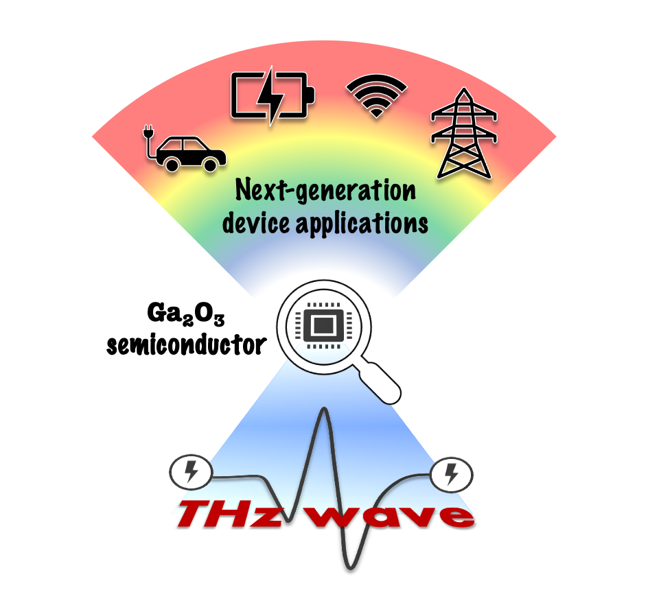
Figure 1. The Ga2O3 semiconductor could pave the way for next-generation semiconductor devices. The use of terahertz (THz) waves to probe semiconductor properties in replacement of conventional yet invasive electrical measurements would accelerate the development of future Ga2O3-based devices and applications.

Figure 2. Frequency-dependent refractive index and extinction coefficient of semi-insulating β-Ga2O3 (left) and doped β-Ga2O3 epilayer (right) along the a crystal axis (E||a) and along the b crystal axis (E||b). The gradual increase in the bulk’s refractive index and extinction coefficient with increasing frequency is ascribed to phonon absorption at higher frequencies. The rapid increase in the epilayer’s refractive index and extinction coefficient with decreasing frequency is due to the effect of free carriers. The Drude-Lorentz model is represented by the black dashed curves. Since β-Ga2O3 is an anisotropic crystal, its complex refractive index differs along different crystal directions. The refractive index is higher along b axis than along a axis. In the epilayer’s case, the anisotropic difference between the two axes in the low-frequency region is relatively small because the refractive index is dominated by the effect of free carriers.

Table I. Material properties of β-Ga2O3 bulk and epilayer evaluated by THz-TDS along with the electrical properties measured by Hall measurement using Van der Pauw configuration. Using the Drude-Lorentz model, the static permittivity and the electrical properties were determined. The static permittivity and refractive index are higher along b axis than along a axis. The electrical parameters are similar along the two axes and the results obtained by THz-TDS are closely comparable to conventional Hall measurements.
Related Links
Technical Glossary
- 1) Gallium oxide (Ga2O3)
Ga2O3 belongs to a group of materials referred to as ultrawide bandgap semiconductors. It exists in various forms, but the most stable one is the β-Ga2O3 crystal structure. Research on β-Ga2O3 materials is a highly active area nowadays because the β-Ga2O3 semiconductor shows significant potential for high-power and high-voltage devices.
- 2) Ultra-wide bandgap (UWBG) semiconductors
Semiconductors are often categorized according to their bandgap – a key property that determines their uses and applications. The conventional silicon (Si) semiconductor has a bandgap of 1.12 eV and is commonly used in integrated circuits. Wide-bandgap semiconductors have a larger bandgap, e.g., gallium nitride (GaN) and silicon carbide (SiC) which have bandgaps of 3.4 eV and 3.26 eV, respectively. Semiconductors with wider bandgaps are used in devices that need to operate at higher voltages and temperatures. UWBG semiconductors are those that have a bandgap larger than that of GaN, like β-Ga2O3 which has a bandgap of ~4.8 eV. Such materials are attractive for high-power and high-voltage applications.
- 3) Terahertz time-domain spectroscopy (THz-TDS)
THz-TDS is a technique that probes material properties using terahertz waves. Unlike ultraviolet light or x-rays, terahertz radiation is nondestructive due to its lower energies. THz-TDS is widely used to characterize the dielectric and electrical properties of semiconductors and other materials in the far-infrared region.
- 4) Terahertz wave (THz wave)
THz waves refer to electromagnetic waves with frequencies in the order of 1012 Hz, specifically in the wavelength region between 3 mm and 30 μm (0.1~10 THz). Aside from their scientific applications like material analysis, THz waves can also be used in technologies such as medical imaging, security screening, and telecommunications. With frequencies higher than radio waves, THz waves can pave the way for high-frequency operation devices and high-speed, ultra-high bandwidth communications. As such, THz is considered key to communication technologies beyond 5G/6G.
- 5) Tera Prospector
Tera Prospector is a general-purpose THz time-domain spectrometer developed by Nippo Precision Co., Ltd. The complex refractive index/permittivity spectra in the terahertz region can be measured accurately using this equipment. In addition to Ga2O3, it can be used for other semiconductors such as Si, SiC and GaN.
https://terahertzwave.com/en/
- 6) Complex refractive index
The complex refractive index is a material property that describes how light propagates through the material. The real part is the refractive index which is related to the speed of propagation, while the imaginary part is the extinction coefficient which indicates how strongly the light is attenuated as it propagates in the material. Light is attenuated when part of the energy is absorbed by the crystal atoms (phonon absorption) or by the free electrons in the material (free carrier absorption). The complex refractive index can also be expressed in terms of permittivity as a function of frequency.
- 7) Drude-Lorentz model
The Drude-Lorentz model quantifies the dependence of the complex refractive index and permittivity on the frequency of light, taking into account the effects of phonons and free carriers. This model is commonly used in evaluating semiconductor materials.
- 8) Static permittivity
The static permittivity refers to the permittivity at zero frequency or 0 Hz.
- 9) Hall measurement
Hall measurement is a conventional characterization technique to measure the electrical properties of semiconductors. In the Hall method using Van der Pauw configuration, current is applied and voltage is measured with the use metal contacts.
- 10) Capacitance-voltage (CV) measurements
CV measurements are another conventional technique used to characterize the electrical properties of semiconductors and devices. In this measurement, voltage is applied then the capacitance of the material is measured with varying voltage with the use of electrodes.
