Electron spin in 2D atomic layers materials induced by orbital angular momentum
A group of researchers from Osaka University, The University of Tokyo, and the University of Wisconsin-Milwaukee (USA) clarified that orbital angular momentum (OAM) induces various spin textures.
Electrons are the primary element of electric current in circular orbits and have a magnetic property known as spin. Electrons rotate and revolve around the nucleus. When the electrons revolve around the nucleus, it leads to the formation of the magnetic moment due to orbital motion and spin of electrons. The effect of the orbital motion of an electron on its spin orientation is referred to spin-orbit coupling (SOC).
When electron spins are aligned, the object becomes magnetized. Thus, electron spin can be considered as electron magnet. When an electron moves in a circular orbit, a magnetic field at the center of the circle is produced, by which the spin vector points toward the center of the circular path.
Electron spin is a major player in next-generation quantum electronic devices that use spin in memory and information processing, so understanding of how to control electron spin is necessary for the realization of novel spintronics devices.
Since two-dimensional (2D) atomic layers materials (ALMs) formed on solid surfaces exhibit broken spatial inversion symmetry, there is a greater electron density, or the concentration of electrons around the nucleus. This electron density produces electrical potential difference in the direction vertical to the atomic layer and induces asymmetrical movement.
It was thought that electron spins appearing in atomic layer crystals originated from the asymmetric density of electrons around the nucleus and that their orientation was perpendicular to both the atomic layer plane and the direction of motion, but the deviations in spin texture from the ideal case were not well understood.
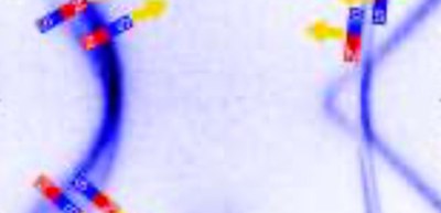
In this study, the researchers measured a Fermi surface (FS) with a novel spin texture in a 2D metallic system formed by indium (In) double layers on silicon (Si) and obtained the splitting: the “circular FS” and the “butterfly FS.” For the circular FS, electrons located in the first In layer moved circularly in the xz plane around the nuclei and produced sizable OAM along the y axis. For the side-part butterfly FS, the electrons located in the second In layer tended to have rotating state in the yz plane.
While the circular movement on the xz plane induces spin along the y axis, the circular movement on the yz plane induces spin along the x axis. Thus, spin on the two FSs can be explained by OAM. From their experimental results and by theoretical calculations, the researchers concluded that the spin texture of the FS of a Si surface covered with two layers of In could be explained by OAM alone, i.e., without invoking the Rashba effect.
Controlling spin polarization and momentum is essential for making devices using electron spin. 2D atomic layers materials become superconducting state. Superconducting computing has potential to overcome the issue of large power consumption due to its extremely low-energy consumption with very high performance. Superconducting quantum circuits are expected to contribute to the development of quantum computers.
Magnet-based memory devices do not consume a lot of energy to memorize information. This group’s achievements will proceed with the realization of energy-saving next-generation quantum devices that allow to gain much information in a short period of time.
Figure 1
Figure 2
The article, “Orbital Angular Momentum Induced Spin Polarization of 2D Metallic Bands,” was published in Physical Review Letters at DOI: https://link.aps.org/doi/10.1103/PhysRevLett.125.176401.
