
Elucidating the phase transition mechanisms of strongly correlated transition metal oxides using the 3D nanotemplate PLD technique
A group of researchers from The Institute of Scientific and Industrial Research (SANKEN) of Osaka University clarified the mechanisms of phase transition, namely metal-insulator transition and insulator-metal transition (MIT and IMT) properties for the electronic domains in Vanadium dioxide (VO2), a typical oxide material that shows huge MIT.
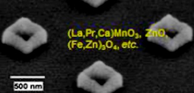
There are many unique characteristics of nanomaterials which do not exist in their bulk form, but as the size of the material shrinks to the nanoscale, the same material may demonstrate radically different properties.
Transition metal oxides (TMOs) are promising candidates for switching memory application because they exhibit reliable and stable switching between a high resistance state and a low resistance state upon the application of weak external stimuli. However, phase-separation through the MIT and IMT is the main reason hampering the understanding of the phase transition mechanism.
In strongly correlated TMOs, nanoscale electronic domains often exhibit an electronic phase separation (EPS) phenomena, so the properties of the metal oxides are determined by nanoscale electronic domains.
A particularly effective approach to identify the phase transition for phase-separated correlated electron materials (CEMs) is to spatially confine the target materials in ultra-small scales equal to the average size of a single domain.
To study the MIT and IMT properties for the VO2 electronic domains, the researchers deposited a VO2 thin film with a thickness of 50 nm on a commercial Al2O3 substrate using the three-dimensional nanotemplate-pulsed laser deposition (PLD) technique that they had developed. They measured the MIT of a single nanoelectronic phase, clarifying the mechanisms of phase transition, such as first-order phase transitions and the TI→M and TM→I distribution in a nanoscale electronic domain.
Devices made from strongly correlated TMOs can be used as an alternative to silicon that can be in a state of 0 or 1 (although the era of silicon seems to be approaching its end), and as intellectual devices like brain chips, which can output multiple values and have selective functions by using the phase transition.
The establishment of techniques to fabricate functional materials with consistent properties will facilitate the development of materials with unique properties and tailored functionalities. The elucidation of nanostructure-property relationships will lead to the development of nanostructure physics and the production of nanoscale devices with more than ten-fold efficiency of conventional semiconductor devices, such as sensors with high sensitivity as well as low-power volatile atomic switches for steep-slope field effect transistor (FET) devices.
The lead author of this article, Hattori Azusa, Associate Professor of the Institute of Scientific and Industrial Research, received the 25th Encouragement Award of the Society of Japanese Women Scientists for her achievements.
Figure 1
Figure 2
The article, “Investigation of Statistical Metal-Insulator Transition Properties of Electronic Domains in Spatially Confined VO2 Nanostructure,” was published in MDPI at DOI: https://doi.org/10.3390/cryst10080631.