
Guiding principles for the manipulation of topological states: Modifying the bulk electronic structure by the charge density wave formation
A group of researchers from The University of Tokyo, the High Energy Accelerator Research Organization, Hiroshima University, and Osaka University has clarified the electronic structure of vanadium ditelluride (VTe2), discovering a change in its topological nature.
While a topological insulator stops current in its interior (or bulk), the currents flow at the edges or on the surface in its topological surface state, showing metallic behavior. Since topological surface states are relatively robust against external disturbances, they are expected to be used for quantum computing and dissipation-less spintronic devices.
A key parameter to characterize the topological nature of materials is band inversion. In bulk materials, the control of the band inversion has been mostly done through the tuning of spin-orbit coupling (SOC) by element substitution and application of pressure and strain. However, since ultrafast switching of the band inversion is difficult to achieve, researchers have intensively investigated methods to conduct the band inversion using various stimuli, such as pressure, electric field, and optical pulse.
The researchers of this group explored topological matters that induce charge density wave (CDW), which can be flexibly controlled by external stimuli, such as electric fields and light irradiation. Specifically, focusing on the transition metal dichalcogenides (TMDCs) VTe2, a well-known family of layered materials that host a variety of CDWs reflecting their quasi-two dimensionality, the researchers made single crystals to investigate the electronic structures of the bulk and surface of VTe2 by employing spin- and angle-resolved photoemission spectroscopy (ARPES).
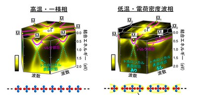
In experiments, they found that on a single-domain without CDW, the Dirac-type topological surface states existed in addition to the V-shaped bulk bands. Thorough three-dimensional investigation of bulk states indicated that the corresponding band inversion dissolved upon the CDW formation, by transforming into anomalous flat bands. The band structures were in a good agreement with their calculations obtained by first-principles calculations.
When the researchers measured on the CDW domain, the V-shaped band transformed into an unusually flat band and the Dirac-type spin-polarized topological surface state was vanished. They analyzed a wave function for this bulk state transformation and found that three major parts of partial density of states (PDOS) were indicative of three bands, arising from the trimerization-like displacements of three adjacent vanadium atoms formed by the σ-bonding of dYZ/dZX orbitals. The two sides of the Fermi surfaces composed of dYZ/dZX orbitals turned into the localized flat bands as a consequence of the vanadium trimerization.
This group’s results show that CDWs induce the drastic directional modification of electronic structure.
Considering that CDWs are often flexible to external stimuli, topological matters that induce CDWs can be utilized for ultrafast manipulation of the topological states. This group will examine new topological matters that induce CDW as well as responses of bulk and topological surface states when external fields are applied.
Figure 1
Figure 2
The article, "Switching of band inversion and topological surface states by charge density wave," was published in Nature Communications at DOI: https://www.nature.com/articles/s41467-020-16290-w.