Osaka solar scientists rough up silicon panels to boost light capture
Osaka University research team modifies the surface texture of both the front and back of silicon solar cells to cheaply enhance light harvesting and boost power conversion efficiency
Power generation cost using solar panels depends on getting as much electricity out of the panels as possible while keeping the manufacturing costs low. Anyone who has considered installing solar panels might be aware of the trade-off between efficiency and the initial cost of the panels. Engineers and researchers are finding new ways to obtain power out of solar modules, but doing so without adding to their costs is becoming more and more difficult.
Now a team of scientists at Osaka University has taken a step closer to making inexpensive solar cells that can deliver the same high efficiency as more complex and expensive cells.
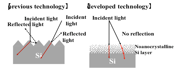
“Unmodified silicon solar cells throw away light energy in the form of reflection, so most solar cells have some kind of antireflective coating,” explains first author Daichi Irishika. “To avoid using these extra coatings we fabricated a submicron structure using a simple wet treatment directly into the silicon surfaces to give the cell its own antireflective coating.”
Antireflective coatings, similar to those used on reading glasses, can help to get more light into solar cells and boost their electricity output. However, these coatings are expensive to produce, especially for covering large areas.
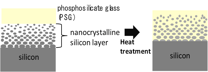
The Osaka team has previously made low reflection silicon cells using a much cheaper process based on the surface structure chemical transfer (SSCT) method to fabricate so-called black silicon. Chemically treating the front side of silicon cells produces tiny submicron silicon structures, which prevent light reflection and give a black appearance. The team has also developed a method to passivate the submicron silicon structures with huge surface area to prevent the recombination loss by deposition of phosphosilicate glass followed by heat treatment. This method can simultaneously form pn-junction to separate photo-generated electrons and holes, and therefore, it isn’t an additional process.
Building on their previous success, the Osaka team turned their attention to the back side of the silicon cells and created rougher light-trapping microstructures to capture even more infrared light.
Group leader Hikaru Kobayashi says, “Making very high efficiency solar cells is important but we should also consider the economics and practicality of any processes used to increase efficiency. The wet processes we have developed are simple yet effective, and our work with black silicon has real-world applications in making cost-effective silicon solar panels.”

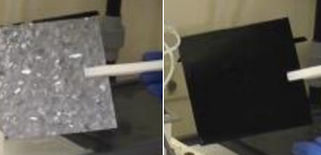
Figure 1. Fabrication of ultralow reflectance polycrystalline silicon wafers by use of the developed technology.

Figure 2. Comparison of low reflectance mechanisms for previous technology and developed technology. (Osaka University)

Figure 3. Developed technology for prevention of recombination of photo-generated carriers in the nanocrystalline silicon layer. (Osaka University)
To learn more about this research, please view the full research report entitled " Improvement of Conversion Efficiency of Silicon Solar Cells by Submicron-Textured Rear Reflector Obtained by Metal-Assisted Chemical Etching " at this page of Solar RRL.
Related links
