
New optical method for measuring surface electric field in semiconductors established
Visualization of surface electric field in solar cells will enhance power conversion efficiency
A group of researchers from the Fukushima Renewable Energy Institute, National Institute of Advanced Industrial Science and Technology (AIST), and SCREEN Holding CO., Ltd., together with the Institute of Laser Engineering, Osaka University, developed a method for measuring the surface electric field in solar cells by combining a technique to measure the shape of terahertz (THz) waves emitted from a surface of silicon substrate by laser light irradiation with a technique to control surface electric field by corona discharge.
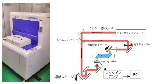
AIST and SCREEN set up a prototype of a laser THz emission microscope at the AIST’s Fukushima Renewable Energy Institute, National Institute of Advanced Industrial Science and Technology in May 2015 to verify its performance. AIST and SCREEN started joint research about enhancement of the power conversion efficiency of crystalline silicon solar cells and methods for assessing their reliability. They demonstrated that it was possible to measure electric fields in semiconductors with the laser THz emission microscope.
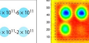
By observing electric fields in the interface between a silicon substrate and an insulating film after spraying ions on insulting films by corona discharge, this group succeeded in quantitatively measuring a fixed charge density in the insulating film in a non-destructive manner.
Generally, there is fixed electric charge, either positive charge or negative charge, in an insulating film composed of silicon dioxide film formed on a crystal silicon substrate, which creates the electric field in the interface between the silicon substrate and the insulating film.
The technique developed by this group does not require attachment of electrodes to samples. It makes it possible to quantitatively measure the fixed charge density at a high spatial resolution in a non-destructive way, regardless of thickness and properties of the insulating film and dope concentration in semiconductors.
The fixed charge density is important information for developing new passivation processes to protect the semiconductor surfaces. This group’s technique is anticipated as a method for measuring interfacial charge of various devices (LSI and power devices) that have insulating film on the surface of semiconductors.
This group will develop crystal silicon solar cells with high power conversion efficiency and measure the fixed charge density of various devices that have the insulating film on the surface of semiconductors. In addition, this group aims for commercialization of a device for measuring fixed charge density by combining a laser THz emission microscope with a corona discharge device.
Details of this technique were presented in the 64th Spring Meeting the Japan Society of Applied Physics Academic Technical that was held at Pacific Convention Plaza Yokohama from March 14, 2017 through March 17, 2017.
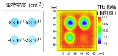
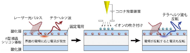
Figure 1
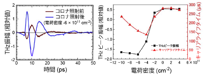
Figure 2
Related link
- Institute of Laser Engineering, Osaka University (link in Japanese)