
New methods for evaluation of wide-gap semiconductors
Visualize defects and surface potential of GaN using THz emission
Wide-gap semiconductors such as gallium nitride (GaN) are widely used for optical devices such as blue LED and are also anticipated as materials for next-generation energy saving power devices and solar cells. However, the quality of GaN crystals does not come up to that of conventional semiconductor materials such as silicon (Si) and this prevents GaN from being used for power devices.
For that reason, the establishment of technology for producing high-quality crystals with fewer defects and rearrangement is expected, and the development of a new evaluation technology is crucial.
A group of researchers led by Iwao Kawayama, an associate professor of the Institute of Laser Engineering at Osaka University, in cooperation with Screen Holdings Co., Ltd., succeeded in visualizing changes in defect density on the surface of GaN through the laser terahertz emission microscope (LTEM) which measures THz waves generated by laser emission. This group’s discovery shows that LTEM is useful as a new method for evaluating the quality of wide-gap semiconductors and it is also expected that LTEM will bring a breakthrough in the development of next-generation optical devices, super high frequency devices, and energy devices.
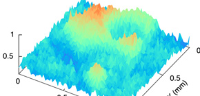
The group examined the intensity distribution of THz generated by radiating ultraviolet femtosecond laser pulses on the surface of GaN crystal through LTEM. As a result, it was found that there were regions with high intensity of THz emission and ones with low intensity of THz emission.
Additionally, when the LTEM image was compared with the image obtained through photoluminescence (PL) using a conventional method, it was found that there was a strong correlation between the distribution of emission intensity due to lattice defects and the intensity distribution of THz wave emission.
Furthermore, from results measurement through modification of excited lasers, it was confirmed that THz emission needs excitation light with larger energy than the band gap energy.
This research was featured in the electronic version of Scientific Reports (UK) on September 9, 2015.
As shown in Figure a, in the neighborhood of the surface of semiconductor of GaN, the energy band is bent due to the surface potential. It is thought that photoexcited carriers are accelerated by the band bending, thereby radiating THz. It is also thought that the change in THz wave emission intensity due to defects, as shown in Figure b, is because the energy band bent significantly due to electrons trapped by defects near the surface, which further accelerated carriers. This shows that LTEM is effective for measuring the defect density of the surface of wide-gap semiconductors and their distribution of the surface potential.
Abstract
Wide-gap semiconductors have received significant attention for their advantages over existing semiconductors in energy-efficient power devices. To realize stable and reliable wide-gap semiconductor devices, the basic physical properties, such as the electric properties on the surface and at the interface, should be revealed. Here, we succeeded in visualization of terahertz (THz) emission from the surface of GaN using a laser terahertz emission microscope (LTEM). We found that the THz emission is enhanced by defects, and this phenomenon is explained through the modification of band structures in the surface depletion layer owing to trapped electrons at defect sites. Our results demonstrate that LTEM is a feasible tool to evaluate the surface potential in a GaN surface. Moreover, this method enables evaluation of the distribution of non-radiative defects in principle, which are undetectable with photoluminescence, and it contributes to the realization normally-off GaN devices.
Figure: a. Schematic illustration of the THz emission mechanism on a GaN surface. b. Schematic illustration of the difference between the band structure in the low defect density region and in the high defect density region on the GaN surface.
To learn more about this research, please view the full research report entitled “Visualization of GaN surface potential using terahertz emission enhanced by local defects” at this page of the S cientific Reports website.
Related links