
Advanced Photoassisted Atomic Switches developed
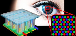
Step in the development of artificial retina and image recognition systems with capacity to learn
A group of researchers led by TANAKA Hirofumi (Assistant professor) and OGAWA Takuji ( Professor, Graduate School of Science, Osaka University) in cooperation with a group led by YANAGIDA Takeshi (Associate Professor, Institute of Scientific and Industrial Research, Osaka University) jointly succeeded in developing intelligent retina switches using photoassisted atomic switches (PASs).
Previously the PAS technology used by these groups only made it possible for a PAS to turn on in response to optical stimulation; it had not been possible to make the switch turn off once it had turned on. The technology the group reports about here has made it possible for them to develop a PAS capable of repeated switching on and off. This technology will make it possible not only to view motion, but also to remember and recognize images that appear most frequently.
Recognition will be conveyed with a minute electric current, so it is expected that this technology may eventually lead to the development of artificial retina operated in conjunction with the electric potential in the human body and that it will make possible an image recognition system with learning function for remembering frequently appearing images or human faces.
Abstract
Using inorganic materials to fabricate synapse-derivative devices is a very important step towards producing neural computing systems. Atomic switches have attracted attention because of their synapse-like behavior exhibiting an ability to switch on and off. If photoresponsive properties can be added to atomic switches, photoassisted atomic switches (PASs) and photosensitive neuron systems such as “intelligent artificial retina devices” can be achieved in the near future.
PASs are atomic switches produced using photoconductive organic materials. Although PAS devices are promising for achieving functional atomic switches, the use of solid photoconductive materials and lithographically patterned electrodes to form a ~100-nm Ag conductive bridge may degrade PASs because it is difficult to compensate for the formation of voids during the rupturing of the Ag bridge. In that regard, the use of (i) nanoelectrodes and (ii) molten photoconductive materials may solve this problem by minimizing the number of voids that are produced and instantly compensating for them. Here, we used self-assembled ITO nanowires as transparent nanoelectrodes to demonstrate stable PAS events. The molten organic molecule 3,4,9,10-tetradodecyloxycarbonylperylene (TDPC) was used as an alternative photoconductive material.
Using ITO nanowire electrodes and the molten TDPC photoconductive material, we can use light to fluently control the change in the amount of current flowing between the ITO nanowire electrode and the Ag2S/Ag electrode. The change in the amount of current flowing between the ITO nanowire electrode and the Ag2S/Ag electrode are obtained when the electrode is subjected to an appropriate bias voltage and irradiated under light. The rapid increase in current indicates that the Ag conductive bridge contacts with the nanowire electrode. The rupture of the Ag conductive bridge can be controlled by applying the opposite bias voltage to the electrode and irradiating it under light. This finding implies that fluent control of the formation and rupture of the Ag conductive bridge at the initial state can be achieved using nanoelectrodes and molten photoconductive material to minimize the volume of voids that are produced and immediately compensate for them. The continuous switching of PAS is used to demonstrate how the photoconductive material compensates for the voids. In addition, the length of the ITO nanowires played a crucial role in the switching behavior of the PAS.
Since controlling the formation and rupture of the Ag conductive bridge at both the initial state and switching required the electrodes to be subjected to a bias voltage and irradiated under light, the introduction of various molten photoconductive materials with different absorption wavelengths into the gap between the ITO nanowire and the Ag2S/Ag electrode to obtain a functional atomic-switch device that exhibits wavelength-dependent photoassisted formation of atomic switches might soon be accomplished. Thus, integrating PAS with various photoconductive materials is promising for the development of a photosensitive neuron system such as an intelligent artificial retina device. Thus, we believe that the knowledge obtained here would be of general interest to the diverse researchers.

Figure 1

Figure 2

Figure 3

Figure 4
To learn more about this research, please read the full research report entitled " Advanced Photoassisted Atomic Switches Produced Using ITO Nanowire Electrodes and Molten Photoconductive Organic Semiconductors " at this page of the Advanced Materials website.
Related link :