
New process to increase semiconductor productivity using EUV lithography developed
A group of researchers led by Assistant Professor OKAMOTO Kazumasa at the Graduate School of Engineering, Hokkaido University, has been involved in a long-term joint research project at the CORE laboratory in The Institute of Scientific and Industrial Research, Osaka University, since the 2015-2016 academic year.
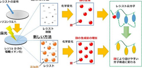
This group, which is involved in study of nanostructure formation at this laboratory, succeeded in developing a new method for drastically improving processing of resist materials used for semiconductor fabrication. Resist performance is evaluated in terms of resolution, line-width roughness, and sensitivity. However, there was usually a tradeoff between them: increased sensitivity worsened resolution and line-width roughness. So the development of new resist materials that break the tradeoff between them has been sought after.
This group developed new technology for increasing sensitivity two-fold or more without worsening resolution and line-width roughness by adding additives to chemical amplification resists that are currently used for semiconductor fabrication. This will lead to the improvement of semiconductor productivity by using lithography such as Extreme Ultraviolet Lithography (EUV) lithography.
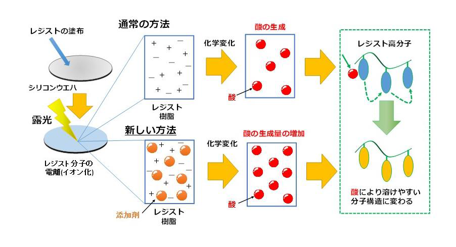
Figure 1
Related link