
A technology for pressureless sinter joining for next-generation power semiconductors
Will add impetus for downsizing power converters at a low cost
Silver micron-particle sintering joining technology developed by Professor SUGANUMA Katsuaki at The Institute of Scientific and Industrial Research, Osaka University, is promising for next-generation power semiconductor, GaN. By improving silver paste, he has developed low-temperature pressureless die bonding, which can be used for all types of electrodes, including Cu and Au, as well as silver coating. These achievements have enabled low-cost, reliable heat-resistant mounting technology for die attach and for printed wiring without changing a conventional cheap electrode structure.
Silver micron-particle sintering joining technology developed by Prof. Suganuma has enabled low-temperature and pressureless die bonding in an ambient environment at a low cost. Because this technology showed high reliability at high temperatures over 250°C, its use is spreading throughout the world as a next-generation main power semiconductor die bonding technology. Although his group clarified the nano-level bonding mechanism last year, the material of electrodes was limited to silver (Ag), because the key to that technology was based on interactions between Ag and oxygen (O).
Nickel/gold (Ni/Au) or copper (Cu) are often used for electrodes for silicon (Si), silicon carbide (SiC) and gallium nitride (GaN) semiconductors as well as direct bonded copper (DBC) substrates. Thus, bonding to Ni/Au or Cu electrodes is in high demand in the semiconductor industry, and the film bonding will expand the scope of its application significantly.
In order to solve these electrode-related challenges, in joint research with Daicel Corporation, this group has developed a solvent to promote interfacial activation of Ag, achieving pressureless sintering technology of joining various electrodes even at 200°C, lower than that of conventional technology. With this new type of solvent (paste), a low electrical resistivity of 4×10 -6 Ωcm, about two times of that of Ag, was achieved, which can only be obtained with Osaka’s-silver paste.
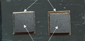
In conventional power semiconductor fabrication processes, films (or sheets) are often used instead of paste as a die attach material. This group developed technology to activate the surface of an Ag film by grinding it. The introduction of this processing formed abundant hillocks on the surface of the Ag film at temperatures ranging from 200 to 250°C, demonstrating that this would lead to the development of new film bonding technology. ( Figure 1 )
This group’s research results will enable not only high performance die bonding of next-generation power semiconductors like SiC and GaN, but also wiring according to surface roughness of a die with lower noise, by no load and low temperatures process. This will achieve the reduction of energy loss during power conversion, which is characteristic of SiC and GaN power semiconductors. This also downsizes power converters, greatly contributing to energy saving and reduction of CO 2 gas all over the world.
This research was conducted as part of the Advanced Low CArbon Technology Research and Development Program (ALCA) of the Japan Science and Technology Agency (JST).
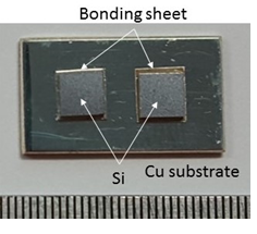
Figure 1. Si die attach example to a lead frame – Si dies affixed to a lead frame using Ag films after treated at 250°C.
Related links