
Technology for 3D wiring of next-generation power semiconductors at low cost developed
A group of researchers led by Professor SUGANUMA Katsuaki at The Institute of Scientific and Industrial Research, Osaka University, developed technology for performing high-performance 3D wiring of next-generation power electronics by silver nanoparticle sintering technology, which had also been developed by this group.
Silver nanoparticle sintering technology is technology for bonding different materials using Ag nanoparticles, which was developed by Professor Suganuma in 1983. It features bonding materials in the atmosphere at a low temperature of 250 °C . This technology has drawn attention as mounting technology for next-generation power semiconductors and its practical application has already begun in Europe. However, how silver nanoparticle sintering was performed at a temperature lower than the melting point of silver, 962 °C, was not known.
This group clarified that a mechanism behind low temperature silver nanoparticle sintering was Ag nano-volcanic eruption and demonstrated that metal sintering went on due to interactions between Ag and oxygen (O) in the atmosphere at a temperature of about 200 °C . This phenomenon occurs only in silver, not in other metals such as gold and copper. Silver has the best electric and thermal conduction, so it is the best material for die attach and wire bonding.
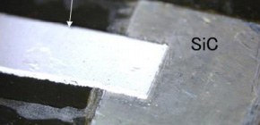
This group performed wiring according to roughness of the surface of SiC die on a substrate via inexpensive printing method and performing calcination of wire forming in an ambient environment without additional pressure at 250 °C , realizing a low resistance of 5×10 -6 Ωcm.
Compared to conventional wiring methods such as wire bonding and ribbon bonding, this new technology using low temperature calcination makes it possible to achieve 3D wiring with lower noise, by no load, and at lower cost.
It is expected that this group’s achievement will improve performance of SiC and GaN power semiconductors and lower their manufacturing costs, promoting downsizing of power converters for power semiconductors and further energy saving.
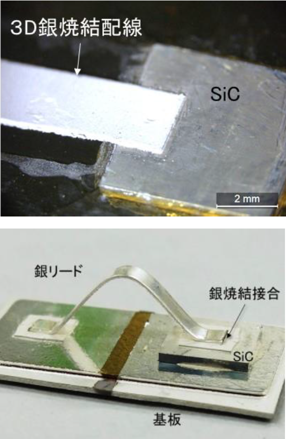
Figure 1
Related link