
High-accuracy AD conversion by optical technology achieved
Possible applications to super high speed optical communications and space/environment observation
A group of researchers led by KONISHI Tsuyoshi , Associate Professor, Graduate School of Engineering, Osaka University achieved seamless operations with below 100-fs jitter (the deviation from true periodicity of a presumed periodic signal in electronics and telecommunications) in an analog-to-digital (AD) conversion at a high accuracy by making use of optical technology, a world first. It can be said that we've reached the starting line for the establishment of next-generation technology after the current electric AD conversion performance reached its limit. This technology will address concerns over electric consumption, which is expected to increase due to the high performance of AD conversion used in various areas such as optical communication, contributing to the development of a rich and sustainable environmentally-friendly society. Furthermore, in the fields of space and environment observation as well, this technology will likely enable information processing of a large amount of data such as super-high-quality movies in broadband optical communication, which is gradually approaching its capacity, as well as measurement of black holes, data which is difficult to obtain.
Abstract
We experimentally realize seamless operations with below 100-fs timing jitter in a 10-GSample/s 3-bit photonic analog-to-digital converter (ADC) with an input 2.5-GHz sinusoidal electrical signal. To address the energy efficiency, it is necessary to explore some serial approaches to get most operations in a photonic ADC done before serial-to-parallel conversion to save the number of devices. To press forward with the work on subsequent operations after optical sampling in a photonic ADC, we have investigated optical quantization and coding and demonstrated their performances. The experimental results successfully demonstrated seamless operations in a photonic ADC, i.e., sampling, quantization, and coding, while keeping its parallel-configuration-free characteristics and low timing jitter below 100 fs. This demonstration could address the energy efficiency by reduction of the number of devices, including electrical ADCs for subsequent operations after optical sampling in existing high-performance photonic ADCs.
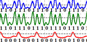
Figure 1. Seamless All-Optical Operations in 10-GSample/s 3-bit Photonic Analog-to-Digital Conversion
Figure2. Digitized 3bit codes after 10-GSample/s 3-bit Photonic Analog-to-Digital Conversion
Figure3. Timing jitter characteristics of quantized signals
To learn more about this research, please view the full research report entitled " Below 100-fs Timing Jitter Seamless Operations in 10-GSample/s 3-bit Photonic Analog-to-Digital Conversion " at this page of the IEEE Photonics Journal website.
Related links