

Generation of electrically-driven single photons in diamond LED at room temperature
a world first!
Synopsis
Under leadership of Associate Professor MIZUOCHI Norikazu , Osaka University, and Associate Professor YAMASAKI Satoshi of the National Institute of Advanced Industrial Science and Technology, a team of researchers succeeded the realization of a stable, room-temperature, electrically driven single-photon source based on a single neutral nitrogen-vacancy center in a novel diamond diode structure -- a first-in-the-world research result.
The results of this research were published online on April 15, 2012 here at nature.com.
Quantum cryptography is expected to be an ultimate, theoretically unbreakable, communication technology and many companies in the world are engaged in its research and development.
To realize this technology, there is a need for a single-photon source that easily and without failure produces single photons for carrying information. However, single-photon sources using quantum dots or organic molecules do not emit light at a room temperature, so cooling to cryogenic temperatures has been necessary. Even the production of a single photon at room temperature required a laser for photoexcitation. So energy and cost constraints were a bottleneck for practical use and diffusion of a single photon source.
This group noticed that the nitgrogen-vacancy center (N-V center) in a diamond emits a stable photon at room temperature and tried driving it with an electric current using N-V center as a single-photon source. (Figure 1)
Specifically, using an advanced manufacturing technology, this group created a light-emitting diode (LED) device by sandwiching a high-quality light-emitting thin diamond region between p- and n-doped diamond layers. Furthermore, through an accurate measuring method such as a photon correlation method, this group verified--for a world first--that the device was electrically driven as a single-photon source at room temperature. (Figure 2)
By combining world-top technologies, the problems associated with cooling a photon source to cryogenic temperatures and the use of a laser, the bottleneck to a single-photon source, could be solved, opening a path to energy-saving and cost-cutting in quantum-communication systems. Further integration of devices will speed up system performance and enhance efficiency. Following verification tests, this new technology will be used for communication of national secrets and private information in the near future.
Additionally, the an excellent function of the spin of the N-V center can be harnessed for improved technologies. That is, this research achievement will contribute to not only quantum cryptography communication, but also to the development of devices necessary for quantum computers and quantum calculations by electrically manipulating spin and photons at room temperature.
This research result was published on online news at the web site of British science magazine Nature Photonics on April 15, 2012 GMT.
This research achievement was obtained through the project noted below.
- PRESTO, Strategic Basic Research Program of Japan Science Technology Agency (JST), " Materials and processes for innovative next-generation devices " headed by SATO Katsuaki, Professor emeritus, Tokyo University of Agriculture and Technology
- Research project " Quantum information devices by single paramagnetic color center in wide-bandgap semiconductor "
- Researcher: MIZUOCHI Norikazu, Associate professor, Graduate School of Engineering Science, Osaka University
- Research venue: Graduate School of Engineering Science, Osaka University
- Research period: From January 2009 to March 2012
This research field aims to create innovative next-generation devices besting existing silicon devices such as CMOS (Complementary Metal Oxide Semiconductor). This field includes innovative research projects to develop new materials and processes, enabling high-speed processing, accumulation, and transmission of large scale information while considering environment and energy consumption.
Background
With the internet being commonplace now, safer communication is much in demand. Current public key cryptosystems will be able to be deciphered through future technological progress. On the other hand, in quantum cryptography, information is transmitted by photons one by one. Therefore, even if in the presence of eavesdropping, eavesdropping will be surely detected by the receiver through the basic principle of quantum mechanics that any eavesdropping would leave traces. Thus, the realization and diffusion of quantum cryptography communication is expected to become the ultimate cryptographic communication method, making eavesdropping theoretically impossible.
Furthermore, it is considered likely that this type of communication will in the future significantly reduce electrical requirements over those of current communication. Some overseas venture companies have already started selling basic systems of quantum cryptography. Also, in Japan, many companies are interested in this technology and are involved in basic technology development and transmission experiments.
In conventional quantum cryptography transmission experiments, mainly artificial single-photon sources with laser weakened to the utmost limit have been used. These artificial single-photon sources can create pulses that contain more than one photon, making them vulnerable to eavesdropping. For this reason, the realization of a single-photon source that produces only one photon in each pulse is being awaited. However, single-photon sources using quantum dots or organic molecules have not emitted single photons at room temperature, so cooling to cryogenic temperatures was essential. And even if a single photon were generated, it would need to be pumped with a laser for photoexcitation. Therefore, energy and cost constraints were bottlenecks to practical uses and diffusion of of single-photon sources.
This group, by making use of single emission centers (N-V center) in diamond as single-photon sources, succeeded, for the first time in the world, in verifying the generation of single-photon source at room temperature in an electrically driven solid-state device that requires high integration and energy-saving for practical use. (Figure1)
Findings
In order to observe only one N-V center, the N-V center needs to be embedded in a high-quality diamond layer without impurities; however, undoped diamond is an insulator. So electricity does not flow in diamond (i-layer) without doping. The important point in this research is that this group created a device with p-i-n structure by sandwiching high-quality diamond (i-layer) between phosphorus-doped "n-layer " and boron-doped "p-layer " (Figure 2), allowing electric current to flow in the i-layer.
Using the group-constructed confocal microscopy, each N-V center was optically detected. Figure 3 (a) is a fluorescent image showing emission from a single N-V center induced by photoexcitation and Figure 3 (b) is a fluorescent image showing emission from an electrically-driven single N-V center at the same position. These figures show that, in case of the electrically-driven single N-V center, emission occurs at the N-V center just as it does in the case of photoexcitation. An antibunching observed by photon correlation spectroscopy verified the emission from the N-V center, showing the N-V center works as a single-photon source. (Figure 4)
This group focused on N-V centers in diamond which emit stable single photons at room temperature. This research result was obtained thanks to high-quality diamond semiconductor combining technology and device manufacturing technology developed by the National Institute of Advanced Industrial Science and Technology and the observation technology of N-V centers developed by Osaka University.
Future development
This research verified a single-photon source is driven not by laser but by electricity at room temperature and that did not require cooling to cryogenic temperatures. It raised the possibility of the birth of energy-saving and low-cost integrated circuits.
The group will improve electric and optical features by optimizing doping conditions, device manufacturing process, and device structure in order to increase communication speed and control emission of single photons in the future. Additionally, in order to achieve long distance communication for quantum cryptography, the emission wavelength should be converted to a 1.5 micron band. In this case, wavelength can be changed with quantum information retained by quantum wavelength conversion devices that have been realized recently. The development of faster and more efficient cryptography communication systems and their verification will make possible the security of communication of national secrets and private information in the near future.
N-V centers also have excellent spin features. Spin can be used for calculation and recording quantum information. Therefore, the development of long-distance quantum cryptography communication using these features and quantum repeaters necessary for high speed communication are also expected. In this case, N-V center is expected to play not a role of a single-photon source but a role of a quantum repeater.
This research result indicates the possible development of quantum information devices that will lead to the realization of quantum computers with quantum registers and quantum memories, and quantum measurement.
Note
In this research, the group created LEDs with help from Research project "Research for Ultra-Low Loss Power Devices" (project leader: YAMAZAKI Satoshi) in the Team Type Research of JST Strategic Basic Research Programs, Core Research for Evolutionary Science and Technology (CREST),"Creation of Innovative Technologies to Control Carbon Dioxide Emissions" headed by YASUI Itaru, Director of the National Institute of Technology and Evaluation and Vice President Emeritus of United Nations University.
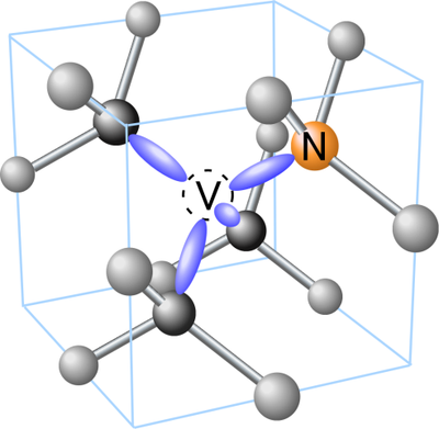
Figure 1
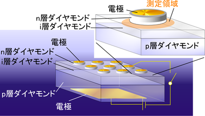
Figure 2
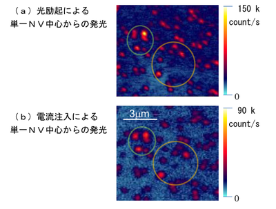
Figure 3
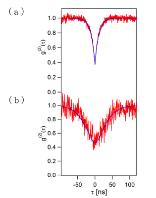
Figure 4
Thesis title : “ Electrically driven single photon source at room temperature in diamond ”
Related link: